Contents
Bare PCB Manufacturing Process
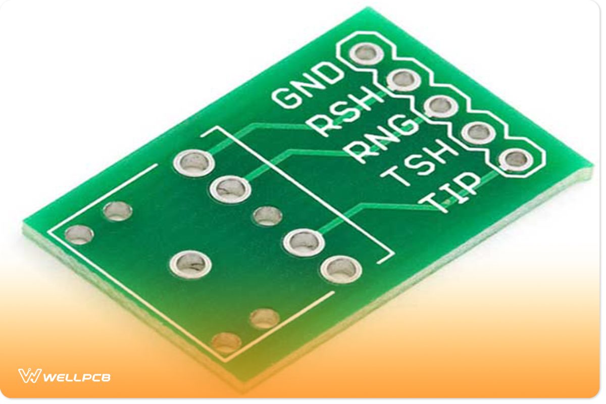
The inventions keep popping up in all computational electronics, including calculators and digital clocks. Printed circuit boards have become a significant backbone in electronics. They are the paths that tell electricity where to go in a circuit. Their work is to direct current on the surface of a board through copper pathways.

Designing Bare PCB
Before designing your bare PCB, it is recommended that you talk to PCB manufacturers. This is critical since it helps to prevent unnecessary errors. Here is an empty PCB manufacturing process.
Step 1.The Design and Output
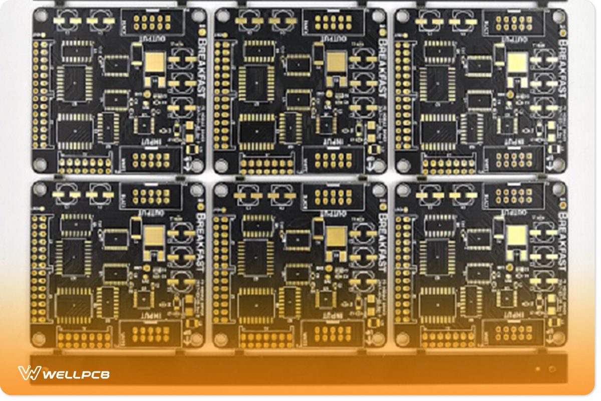
The circuit board you come up with should be rigorous and must have a layout designed by software. To this end, you may use software such as KiCad, OrCAD, Altium Designers, or Eagle. Your manufacturer will want to know the version of software used in designing the circuit. This is important since it helps to reduce discrepancies.
After the approval of the PCB design, you will need to export the design into a format supported by the manufacturer. The design is then converted into an output format. This could be done using the extended Gerber. It encodes vital information such as tracking layers, component notations, apertures, and so forth. All PCBs will then have to undergo checks which ensure that no errors are detected. You will then need to plan on other elements such as track width, trace hole spacing, board edge spacing, and the size of the hole. The file should then be forwarded to the boarding house for production. However, the design must fulfill the minimum tolerance requirements.

Step 2. The designer needs to output the schematic files, which the manufacturer will use to make photo films.
These films will then be used to image the PCBs. To do this, the designers may choose to use plotters to help provide a detailed PCB design.
At this point, you will then have a plastic sheet with a negative film for your PCB. The negative photo will be in blank ink and represent conductive copper parts. The plotter will then develop a film layer that can be stored. It also has an outer layer that covers the areas consisting of non-conductive material.
Each PCB layer will have a black film sheet; there should be two solder masks in a two-layer PCB. Notice that you must achieve correspondence of the films. You will need to punch holes through the film to achieve this.

Bare PCB Inspection
Notice that the visual inspection only works when inspecting a two-layer PCB. It is the testing of the printed circuit board. This could be done manually or using automated devices to help find any possible problem. However, in multi-layer PCBs, a visual inspection will not give you the desired results. As such, it may be necessary that you conduct an electrical test.
Electrical Test
Here, you may have to choose between a universal grid and a flying probe. The universal grid requires that you use fixtures in conducting the test, while the universal grid does not require the use of institutions. The universal grid is also referred to as the bed of nails or clamshell test.
Typically, a PCB test could either be capacitance or resistance. The capacitance test helps to detect opens and shorts. At the same time, the resistance test helps to measure the flow of current through traces.
If you have traces of the same material, but one is two times longer than the other, the resistance of the longer one will be two times the resistance of the shorter one.


