Contents
- 1 What Are 3D Printed Circuit Boards (PCBs)?
- 2 How Do 3D Printed PCBs Work?
- 3 What Are the Advantages of 3D Printed PCBs for Electronics Companies?
- 4 What Are the Challenges of Implementing 3D Printed PCBs?
- 5 What Are the Real-world Applications of 3D Printed PCBs?
- 6 What Is the Future of 3D Printed PCBs in Electronics Manufacturing?
- 7 Expertly Integrate 3D Printed PBCs Into Your Manufacturing Processes.
What Are 3D Printed Circuit Boards (PCBs)?
3D-printed circuit boards are either entirely or partially constructed using additive manufacturing. This means that a single 3D printer typically creates the bulk of the PCB.
A lot of complex processes and steps go into fabricating modern PCBs. It’s highly involved, requires expertise from several backgrounds, and is justifiably expensive. Additive manufacturing was introduced to simplify the PCB manufacturing process and make it less costly.
In traditional PCB manufacturing, copper-clad boards are etched or milled to create conductive pathways. However, with 3D printing, manufacturers can either print the conductive pathways directly into a piece of laminate or use mixed-material 3D printers to print both the dielectric and electric components. This eliminates the need for pre-fabricated copper boards, offering greater flexibility in design and material usage.
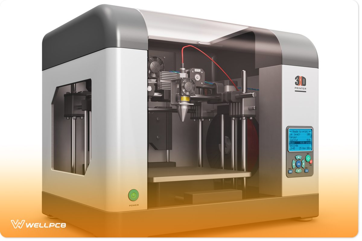
While similar, the 3D printers that manufacturers use to fabricate electronic components (like PCBs) are slightly different from those used by general consumers. Industrial 3D printers are more robust and, in most cases, more powerful.
Types of Industrial 3D Printers for PCBs
The most common industrial 3D printer types for PCBs are as follows:
- Fused deposition modeling (FDM)/ Fused filament fabrication: The most common type of 3D printer, often used in homes. They use nozzles to mold and shape constructs from thermoplastic. Manufacturers can only use them to construct a plastic base or substrate for the PCB.
- Stereolithography (SLA): The oldest type of 3D laser printer. They use lasers to cure resin into solid layers and shapes. Because lasers are more precise than nozzles, manufacturers can use them for more accurate designs. Again, these printers are limited to creating PCB substrates.
- Selective laser sintering/melting (SLS/SLM): Uses lasers to melt and form shapes from polymer powders, including metallopolymers and composites. Unlike the previous two printers, manufacturers can leverage SLS to fabricate the conductive and non-conductive elements of the PCB.
- Material jetting: Based on inkjet technology. However, instead of ink, the machines use liquified polymers. Manufacturers utilize them to create both the substrate and conductive layers of the PCB. Alternatively, it’s ideal for laying down the conductive pathways of the PCB, a technique known as direct writing.
How Do 3D Printed PCBs Work?
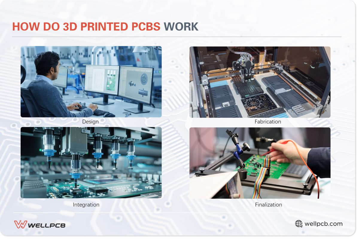
Regardless of the printer type, the 3D printing process follows a similar flow:
- Design: A designer creates a virtual 3D rendering or model of the desired PCB design. Depending on the extensiveness of the 3D printing process, this design can contain the structure, circuitry, and embedded components (if there are any).
- Fabrication: An operator feeds the virtual design into the 3D printer, which then forms the PCB. You can break up this process into phases. For instance, the printer can first create the circuitry, often using conductive and dielectric inks. After that, it might be encased it in laminate material (sometimes using a separate printer). The specific steps really depend on the type of 3D printing.
- Integration: At this point, fabrication of the bare board PCB will be complete. The manufacturer can then assemble the PCB’s electronic components. In some cases, they can use 3D printers to embed select components directly onto the PCB.
- Finalization: To ensure the quality of the PCB, the manufacturer may send it for additional processing. This may include soldering and solder mask application. The PCB then undergoes testing and quality checks to ensure it’s fully functional.
What Are the Advantages of 3D Printed PCBs for Electronics Companies?
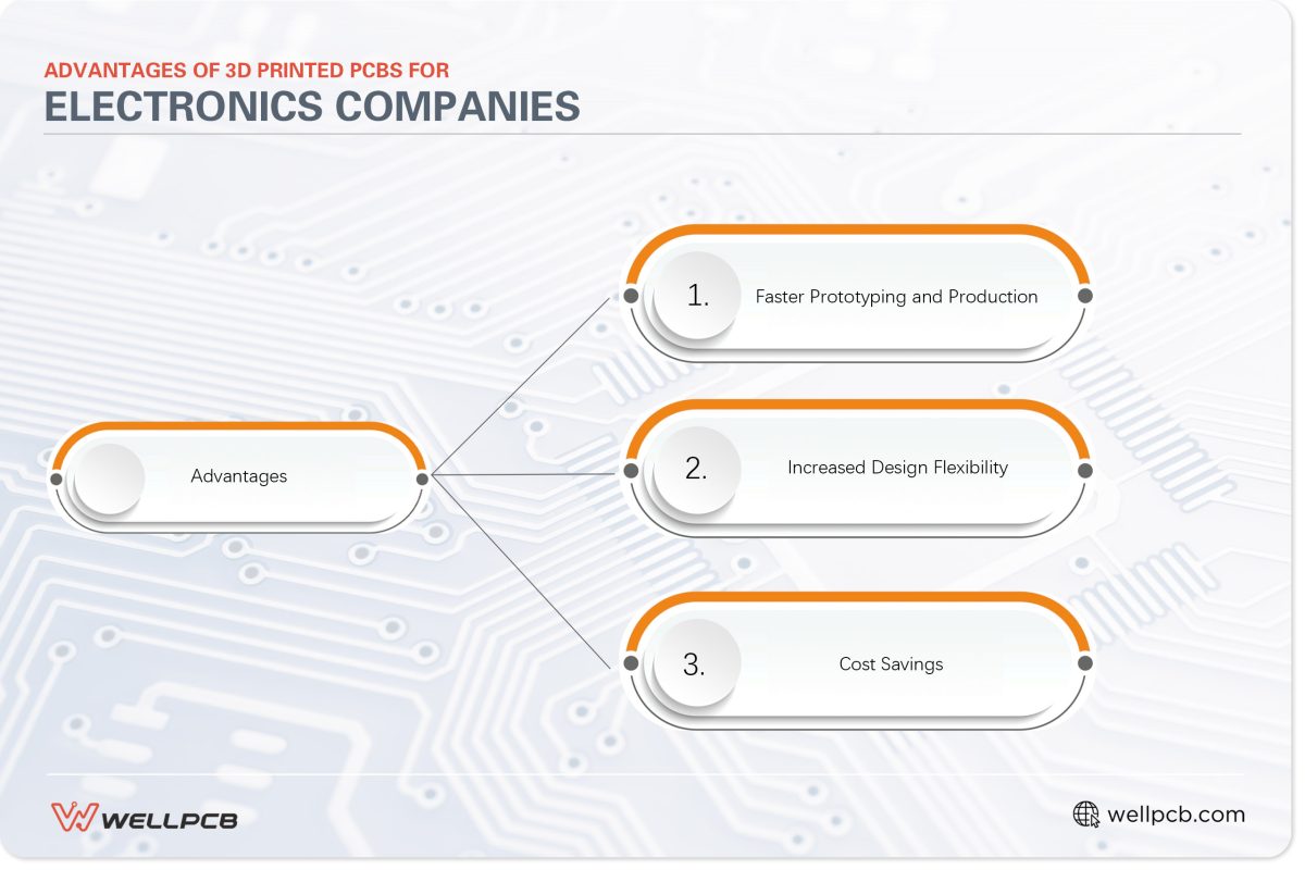
3D printed PCBs offer several advantages to manufacturers and electronics companies. Chief among these are:
Faster Prototyping and Production
Many PCB manufacturers are located in East Asian countries, such as China. It’s pretty commonplace for Western electronics manufacturers to send their PCB designs to these countries for prototyping. The problem with this is that the complexities of overseas production and shipping can result in lengthy lead times.
3D printers allow electronics makers to prototype their designs in-house. This allows them to tweak, improve, and iterate their designs more easily. After finalizing the design, they can collaborate with a PCB manufacturer to mass-produce it.
As a result, the ability to rapidly prototype PCBs on-premise enables electronic companies to shorten the time to market for their products.
Increased Design Flexibility
On-premise 3D printing grants electronics makers more freedom to be creative. They can create custom PCB designs tailored to their unique device requirements.
This is especially beneficial in low-volume productions where traditional PCB fabrication techniques may not be sufficient to fulfill the design specifications.
3D printers allow designers and manufacturers to craft PCBs with intricate structures and geometries.
This includes specialized high-density interconnect PCBs and other multilayer or complex designs.
Cost Savings
While upfront costs for 3D printers can be high, the production and long-term costs are typically lower than traditional PCB manufacturing techniques.
This is because 3D printers use materials more efficiently. They use up less energy and produce less waste.
So, besides cost efficiency, additive manufacturing can also be more environmentally friendly, especially for small-batch productions or homemade printed circuit boards.
What Are the Challenges of Implementing 3D Printed PCBs?
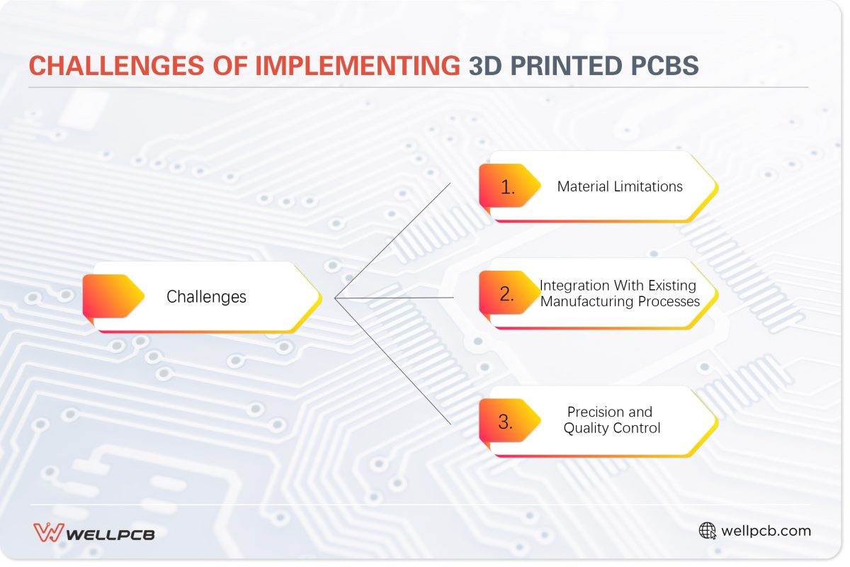
Unfortunately, with all its benefits, additive manufacturing isn’t a flawless technology. At least not yet. There are a few things to consider before committing to it.
Material Limitations
3D printing is only compatible with a limited range of materials. More flexible 3D printing options (such as mixed material 3D printing implementations) tend to be more expensive.
In addition to this, certain 3D printing materials may not perform as well as traditional fabrication materials.
For example, the conductive materials in 3D printed PCBs may not be able to facilitate high-frequency digital signals as effectively as traditionally crafted copper traces.
While 3D printing may still be suitable for prototyping in these cases, conventional PCB manufacturing is more suitable for mass production of high-powered designs.
Another limitation is that although 3D printing materials are flexible, they may not be as durable, strong, or long-lasting as traditional PCB materials. As such, the robustness and longevity of 3D printed PCBs may not match those made using conventional means.
Integration With Existing Manufacturing Processes
Additive printing can be relatively cost-effective when applied in the right scenarios. For instance, manufacturers can save money on prototyping in-house.
The same can be said for small-scale productions where 3D printing eliminates the need for expensive molds, tooling, and setup processes.
When it comes to large-scale production, traditional PCB manufacturing techniques tend to be more cost-effective due to economies of scale.
Once the initial setup is complete, traditional methods can mass-produce PCBs at a lower per-unit cost.
In contrast, 3D printing, which builds each PCB layer by layer, becomes less efficient for large volumes, leading to higher costs and longer production times.
Therefore, integrating 3D printing as part of a broader production strategy—rather than relying on it exclusively—can offer the best of both worlds.
While it won’t completely eliminate the limitations of 3D printing, it optimizes its use, particularly for prototyping and short-run productions.
In any case, you’ll still have to account for necessary post-processing steps, such as curing and surface finishing, which add time and complexity to the production process.
Precision and Quality Control
It can be challenging to fabricate high-resolution designs that require great precision with some 3D printer types.
Often, finer conductive pathways and small meticulous components can be complex to create accurately, especially with FDM/FFM printers.
There’s also the point that 3D printing technology is still in its infancy and hasn’t yet been widely adopted by the PCB manufacturing industry.
As such, there is an unfortunate lack of standardization.
When adopting additive printing, manufacturers are still bound to IPC standards and other industrial regulations.
This can be tricky to adhere to, considering that 3D printing isn’t comprehensively covered under these standards and regulations.
You can address this challenge by collaborating with experts like WellPCB.
Along with integrating the requisite machinery and equipment, training and hiring the required personnel can substantially increase production costs.
Nevertheless, these cost increases can be temporary if you develop a solid manufacturing strategy around 3D printing.
What Are the Real-world Applications of 3D Printed PCBs?
So far, we’ve explored the potential benefits of additive manufacturing for PCBs. Now, we’ll discuss some forward-thinking companies that have managed to reap the benefits of the technology in the real world.
Speeding Up Product Development
PHYTEC, a company that designs, builds, and supplies embedded electronic solutions, uses 3D-printed PCBs to speed up its product development cycle considerably. Like most companies, PHYTEC wanted to decrease their long lead times and reduce costs.
Background
PHYTEC found that the constant need to retool and amend their designs complicated and slowed the design and production processes. This would further delay the product’s time to market, not to mention compound their costs.
Once PHYTEC completed its designs, it would send Gerber files to its partner PCB manufacturer in Europe or Asia. Lead times would be at least eight working days for medium-complexity PCBs. This number could easily rise to 50 days for more complex PCBs.
In addition, PHYTEC had to pay a one-time setup fee between €170 and €500 for every round. If you take express fees into account, this expense could easily double.
Implementation
PHYTEC addressed these challenges by adding an advanced material jetting 3D printer to their tool stack. The printer allows them to workshop their designs at speed, rapidly prototype them, and reduce overall costs.
Outcome
It now takes PHYTEC between 12 and 18 hours to create a prototype of a PCB, which is at least ten times faster than ordering PCBs the traditional way.
Ultimately, integrating the 3D printer allows PHYTEC to enhance its design and development workflow. This, in turn, enables them to shorten production cycles and bring products to market faster.
Customizing Electronics for Niche Markets
BotFactory, a company specializing in desktop PCB printers, developed a new printer to create customized electronics for niche markets.
Background
Traditional PCB manufacturing can be inflexible, expensive, and time-consuming for small businesses and hobbyists. BotFactory aims to address these limitations through its Squink printer. The printer delivers low-scale productions for highly customized PCBs, opening the door to entities and users who previously didn’t have access.
Implementation
What makes the Squink printer so innovative is how it uses inkjet technology to form conductive traces and components directly onto substrate slabs.
Outcome
The Squink printer allows for easy, quick in-house prototyping that is affordable to everyday consumers and startups. By creating an inexpensive and easy-to-use printer, they can meet the needs of niche markets that were previously underserved.
Reducing Waste and Improving Sustainability
Nano Dimension, a 3D printer supplier, is known for helping companies reduce waste and reach sustainability goals through their technology.
Background
Nano Dimension has built a reputation for itself by being at the forefront of innovation in the design and development of industrial 3D printers. One of the company’s goals is to address the environmental impact of conventional PCB manufacturing.
Implementation
Nano Dimension seeks to create less energy-intensive methods to fabricate PCBs and reduce chemical waste. Their solution is the DragonFly 3D printer, a mixed-material jet printer based on inkjet technology.
Outcome
The Dragonfly system fabricates the PCB by expelling both conductive and dielectric materials, layer by layer. In almost a single process, fabrication is complete. Since this process does not require chemical etching or plating, it dramatically reduces chemical and material waste.
What Is the Future of 3D Printed PCBs in Electronics Manufacturing?
At the time of writing, additive manufacturing is an emerging technology. It’s yet to be fully embraced by the industry. However, the future seems promising enough.
Emerging Trends and Innovations
Additive manufacturing is notoriously difficult to automate, but artificial intelligence may soon help address this. With AI at the helm, entire productions can be fully machine-controlled.
The material limitations are another reason the industry has yet to fully adopt 3D printing. However, 3D printer makers continue to develop and introduce new materials, such as conductive inks and polymers.
These materials can potentially improve the mechanical strength and reliability of 3D printed PCBs. They also provide enhanced conductivity and flexibility. Liquid Crystal Polymer (LCP), in particular, is helpful in high-frequency applications.
Potential Impact on the Electronics Industry
3D printing’s ability to promote innovation in the design of PCBs will only positively impact electronics. A review headed by famed economist and scientist C. Hanumanth Rao concluded:
“Though it is improbable that electronics 3D printing will replace all the conventional subtractive processes for the development of high-performance electronic device applications, yet this technology will surely be useful for rapid prototyping with minimized production time and reduced manufacturing costs.
Several research institutes, including UC Berkley and Duke University, are conducting extensive research on printed electronics for the realization of microelectronics and wireless sensors and conductive thermoplastic materials, respectively.”
Multi-material and high-resolution 3D printing will allow us to fabricate more advanced and detailed designs. One day, we’ll be able to print entire PCB assemblies on a single machine.
Expertly Integrate 3D Printed PBCs Into Your Manufacturing Processes.
Early adoption of technology can give companies an edge. However, not all technologies succeed in the long run and are worth long-term commitment.
In our expert opinion, 3D-printed PCBs are promising. Even if the technology fails to proliferate, there are indications that designers, electronic makers, and PCB manufacturers will still use it in some capacity. This is because 3D-printed PCBs can be cost-effective and flexible, helping electronic companies create innovative designs.
Are you interested in integrating 3D printed PCBs into your manufacturing process but don’t know where to start? Contact WellPCB today to explore how 3D-printed PCBs can benefit your company or production.