
Contents
- 1 1. What Are Pre-Layout Guidelines?
- 2 2. What Are the PCB Layout Guidelines for Placing Components?
- 3 3. Which PCB Routing Guidelines Maximize Efficiency?
- 4 4. How Do You Define the Widths of Your PCB Trace?
- 5 5. What Are the Guidelines for Testing Your PCB?
- 6 6. Why Use a PCB Assembly Service Like WellPCB?
1. What Are Pre-Layout Guidelines?
Before diving into the layout guidelines, several factors must be addressed to ensure successful PCB design. These pre-layout guidelines include the following.
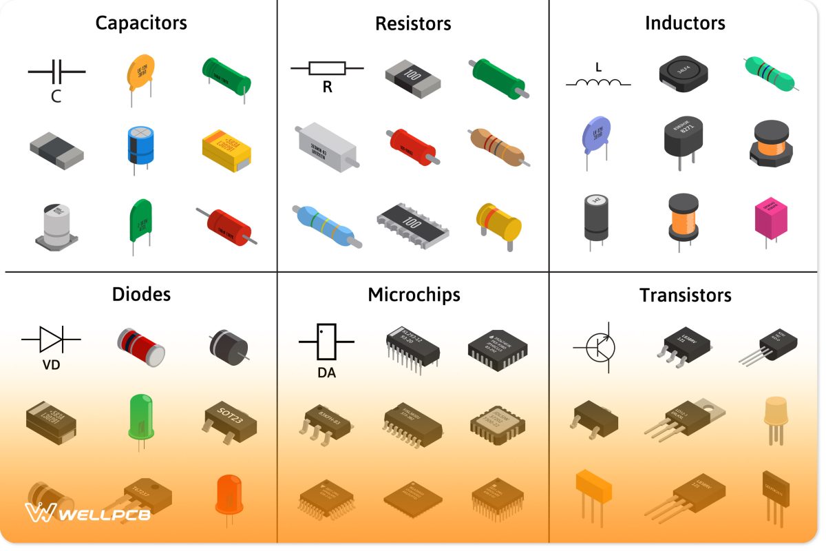
Libraries
Libraries contain details on the board’s land patterns, ensuring specifications are applied consistently throughout the manufacturing process. When developing these libraries, it’s important to use industry standards (such as IPC) or the fabricator’s specifications. Keep in mind that individual, corporate, or technological requirements often call for changes in these libraries.
Generally, you should ensure that all library parts conform to acceptable land pattern sizes per the relevant standards. PCB footprints should include all the necessary elements, such as silkscreen markings and part outlines.
Before finalizing your design, confirm with your fabrication house that they can manufacture these components. Alternatively, you can use an external CAD library vendor’s PCB footprints, as component manufacturers often have different parts built for specific design systems.
Schematics
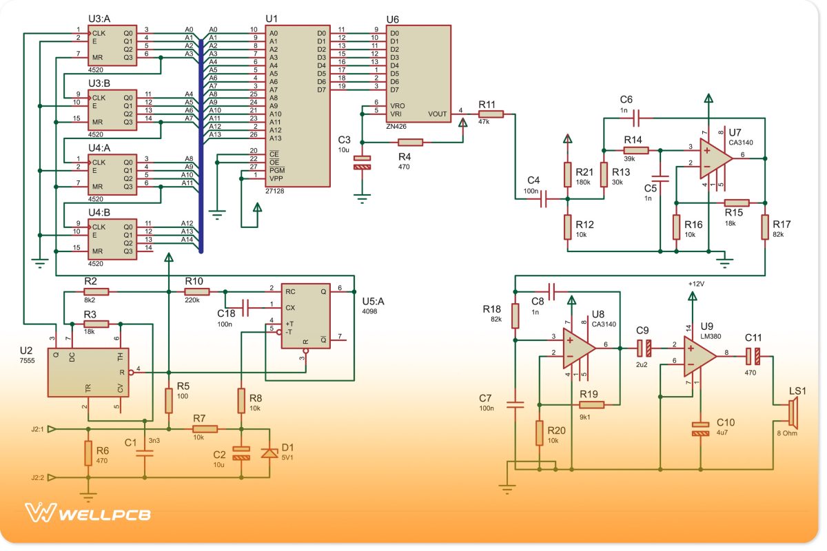
The schematic is the electrical blueprint of your PCB. Common guidelines for schematic development include:
- Logical placement of symbols on schematic sheets
- Comprehensive component data (part number, reference designator, pin number, and value)
- Consistent net object colors (net buses, text, net lines, etc.)
- Clear naming conventions
- Appropriate net spacing
Many companies have internal drafting guidelines that cover:
- Schematic sheet and border information
- Grid size and appearance
- Symbol size
- Text height and font size
- Line widths
The layout process should only proceed once the schematic guidelines have been checked and verified.
CAD Parameters and Settings
CAD systems can be customized to provide more control over fill patterns, colors, font sizes, font width, and shadowing. Rather than using the default parameters, consider how you can adjust these settings to make the layout workflow more efficient.
Board Outline and Stackup
Designing your PCB with an accurate board outline and suitable form factor helps avoid costly and time-consuming redesigns. Ensure the outline has all the required CAD elements, such as keepout zones.
Fine-tune and finalize the board stackup early to avoid later changes that may impact signal routing, like impedance-controlled traces. Consider the board materials carefully, as factors like dielectric constant, dissipation factors, and moisture absorption will all affect your calculations and measurements.
2. What Are the PCB Layout Guidelines for Placing Components?
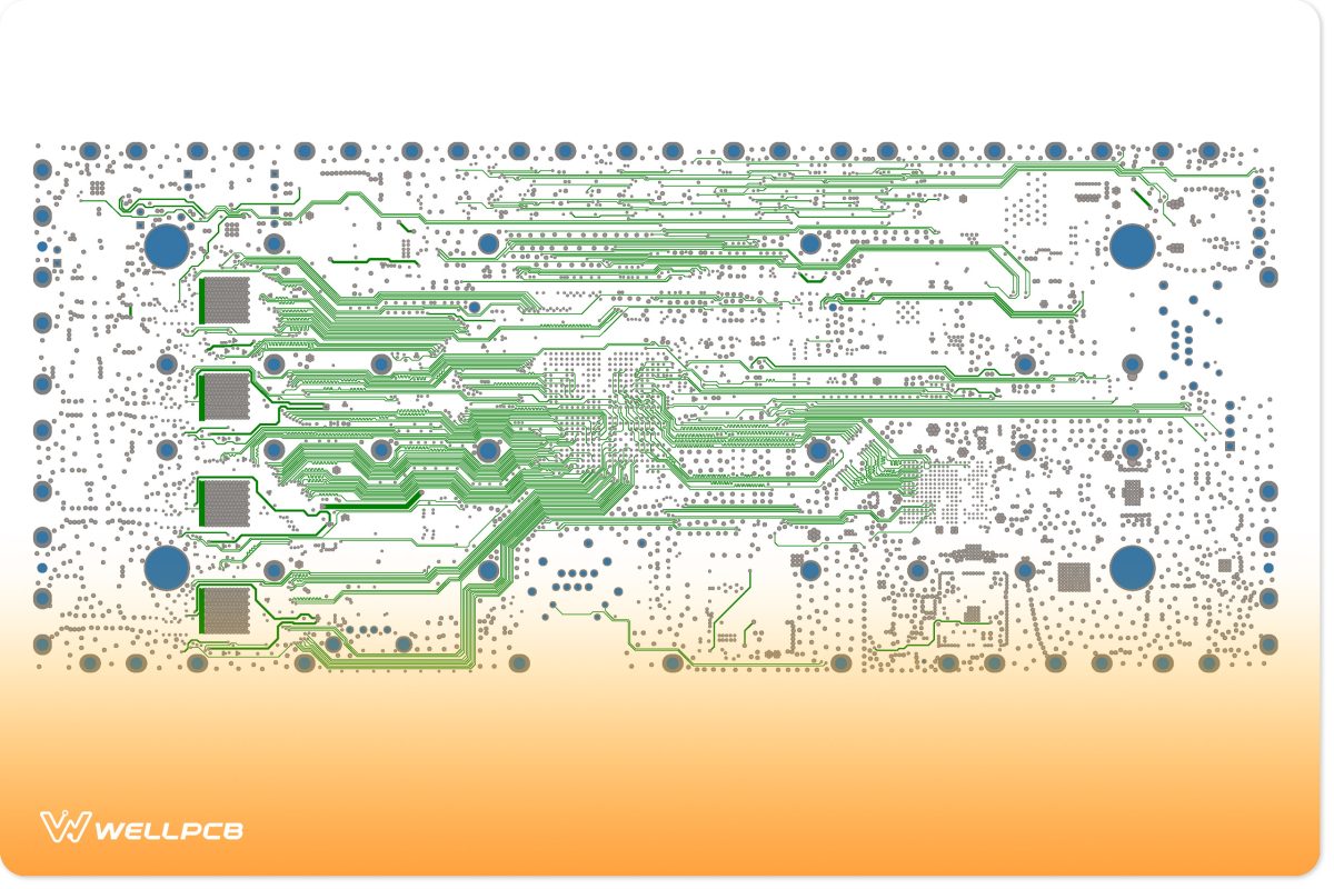
Correct placement of PCB components is vital for optimal performance, reliability, and manufacturability. Here are some best practices for custom PCB layouts:
- Place components in the right order. Placing essential components first, followed by power, ground, and signal traces. Considering their size and mechanical enclosure constraints, essential components must be positioned strategically. In multi-layer PCBs, the power and ground planes should next be placed on the two internal layers. For 2-layer boards, the ground plane should be positioned on one layer, with the signal and power traces routed in the other layer.
- Place large processors and ICs in the middle. High-pin-count chips connect to several components on the PCB, so these need to be placed centrally for easier routing.
- Avoid crossing nets. When placing the components, chips, and traces, minimize the number of crossing nets. Every net intersection adds complexity, as they need vias to transition between layers. Placing components creatively and experimenting with orientation to reduce net crossings will make it easier to follow the best routing guidelines.
- Use thermal relief connections for through-hole components. Ground planes can act as heat sinks, removing heat from all the connected vias. This is problematic when attaching through-hole components using wave soldering, as heat is drawn away from the through-hole. Thermal reliefs are, therefore, essential to maintain the soldering temperature and prevent cold joints.
- Separate high-power components within the design. High-power components emit more heat, so they should be distributed evenly to prevent hotspots.
- Group components strategically. Certain components can be grouped in the design, such as those within the same circuit. As a rule of thumb, group digital components on one part of the PCB and analog components on the other. This will help prevent electromagnetic interference.
Decisions around component placement are also influenced by the requirements of the PCB. Here are some key considerations.
Circuit Performance
For high-speed circuits, keep component distances short to ensure direct signal paths. The same applies to power and analog circuits, as their high-current and sensitive electrical lines should be as short as possible.
Short paths increase power and signal integrity while reducing inductance. However, spacing might be necessary due to thermal issues or to accommodate bus routing.
Accessibility
PCBs require manual testing and reworking, which requires parts to be easily accessible. As such, large components shouldn’t be placed over smaller ones. This also helps to avoid potential collateral damage when accessing adjacent parts.
It’s considered best practice to first develop a basic floor plan of the parts on the PCB, and then plan how to build the various circuitry areas.
Manufacturability
Components should also be placed in a way that facilitates ease of manufacturing, thereby preventing defects and reducing unnecessary costs. Tall chips, for instance, should not be placed next to small components, as this can create a shadow effect that weakens solder joints.
Parts that are too close together can also hamper automated soldering and assembly. Involving your manufacturer early in the design process can help optimize component placement and improve overall manufacturability.
3. Which PCB Routing Guidelines Maximize Efficiency?
Balancing component placement with optimal trace routing is a challenge, especially in high-density designs. The following guidelines can help you achieve efficient routing.
Design Constraints
A significant portion of PCB design rules and constraints apply to trace routing. These govern various specifications, including trace width and spacing for each net, specific net classes (group of nets), or all non-specified nets (default).
Design rules can also specify which vias to use for specific nets and trace lengths. They can additionally determine component spacing, mechanical clearances, and silkscreen rules, along with the board layers that route specific nets and topologies.
Power and Signal Integrity
Efficient trace routing is key to maintaining power and signal integrity. To achieve this, adhere to the following parameters:
- Short and direct high-speed trace routing to minimize signal degradation.
- Controlled impedance routing, with appropriate layer selection, trace spacing, and width.
- Length tolerances for matched length routing, are vital for time-sensitive circuits.
- Optimal spacing and width for sensitive signals, such as clock and control lines.
- Copper weight and trace width for high-current power lines.
- Differential pair routing to avoid crosstalk, with appropriate trace widths and spacing.
- Via selection based on the specific requirements of each net.
4. How Do You Define the Widths of Your PCB Trace?
Trace width is critical in PCB manufacturing, as it affects current handling, manufacturability, and signal integrity. Here’s how to determine the correct width of your PCB trace:
- Current: Traces handling high current values must be wider to avoid overheating from electrical resistance. The width is determined by the current load the trace will handle. For reference, the default trace width for PCB lines is 10 mils but traces carrying more than 0.3A should be wider.
- Manufacturability: Super thin traces can be problematic during fabrication, as the etching process can remove most of the copper in some sections. Therefore, always ensure the trace width is broader than the minimum your manufacturer can handle.
- Impedance: Impedance control only applies to specific nets, such as high-speed RF or digital signal lines. These need a calculated trace width to achieve the required impedance value and maintain signal integrity.
5. What Are the Guidelines for Testing Your PCB?
Most PCB defects can be identified and rectified early in the design process by carefully checking the layout. However, this can be challenging to manage when finalizing the layout for manufacturing.
Electrical Rules Check (ERC) and Design Rules Check (DRC) are two methods that can simplify the testing and quality control process, ensuring the board meets all design rules. Combined, these assessment methods make it easy to define physical requirements, such as:
- Gap and trace widths
- Common manufacturing requirements
- Electrical constraints for high-speed applications
ERC and DRC effectively simplify and accelerate the quality control process, ensuring your design meets all relevant standards. Tools like Sprint-Layout can be used to automate these checks.

6. Why Use a PCB Assembly Service Like WellPCB?
While simple PCB layouts with few layers can typically be handled in-house, complex multilayer designs with high-density components require careful inspection and collaboration with your manufacturer.
At WellPCB, we can streamline this process, helping you implement relevant guidelines to make manufacturing and assembly quick, seamless, and affordable.
We’ll give you access to our engineers and technical team to help fine-tune your circuit’s layout. Alternatively, you can let us handle the entire PCB production process—from design to assembly—at a small extra cost.
Contact us with your project details, and we can work together to chart the best way forward for a successful partnership.