Contents
What is TL494 IC?

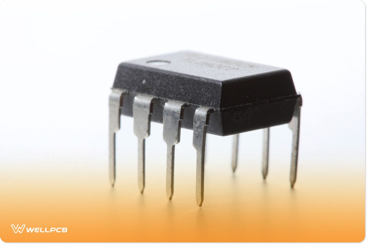
8 Pin PWM controller
TL494 is a PWM controller integrated circuit that you can use for devices with power electronic circuits. It features two on-chip error amplifiers alongside an oscillator for adjusting frequencies, an output control circuit with feedback, and a flip-flop output with a pulse steering control.
The error amplifiers are responsible for compensating voltage between -0.3 to VCC -2V in a standard voltage configuration. Also, the comparator dishes out almost a 5% range by controlling the dead time with a fixed offset.
Further, the external oscillator provides a reference frequency signal for the PWM integrated circuit, while the Internal Regulator delivers a stable 5 V Reference Supply. However, you can always bypass the on-chip oscillator by attaching an RT to the output pin of the reference.
Interestingly, the TL494 is a complete PWM power-control circuitry that you can use for single-end operations. Also, the TL494 is useful for push & pull configurations.
But that’s not all.

PWM Microchip
This PWM control electrical circuitry comes with all the functions you need to design a power supply circuit. Check out the diagram below:

Variable PWM IC with a fixed frequency
The diagram above can vary the pulse width by comparing the sawtooth waveforms of two individual internal oscillators. The timing capacitor holds the internal oscillators on any of the control signals. So, the output becomes high when the control signal goes lower than the sawtooth waveform’s voltage.
TL494 Specifications
- The supply voltage ( Vcc) is up to 41 volts
- The maximum output current for both PWMs is 250mA
- Output voltage at collector pins is 41 volts
- It has a temperature range of -65 to 150 degrees
TL494 Features
- It has an in-built PWM control channel
- 200mA sink or source current
- It has dual output selectable operations, which include Single-ended and push-pull operation
- The TL494 has a variable range deadtime control feature
- You can easily synchronize the TL494 with other circuits
- It has two PWM outputs
- It comes with a fixed-frequency oscillator
TL494 Pinout & Pin Configuration
Here is a table with details of the TL494 pinout and pin configuration:


Internal Structure of TL494 containing all components
Now, let’s take a closer look at the different components that make up the internal structure of the TL494.
5V Reference Source
The reference source of the TL494 is in-built. Plus, it works according to the bandgap principle, and the TL494 has a stable 5-V output voltage. But there’s a condition. The VCC voltage must be above 7V, and the error must be within 100mV. The reference sources use the 14th pin REF as its output pin according to the pin configuration table.
Operational Amplifier

DIP-8 operational amplifier
There are two operational amplifiers installed on the TL494. The two amplifiers get power from one single power supply. The operational amplifier has a transfer function of ft(ni, inv)= A(ni-inv). However, this transfer function doesn’t exceed the output swing.
Each operational amplifier has an output terminal that you can connect to a diode. Plus, the diode serves as a bridge between op-amps and the subsequent circuit. So, the diode, when connected to the COMP pin, ensures the op-amp with higher output enters the following circuit.
Sawtooth Oscillator
Perhaps one of the best selling points of the TL494 is its built-in sawtooth wave oscillator. The sawtooth oscillator generates a sawtooth wave of 0.3 – 3V. Also, you can adjust the oscillation frequency by using an external resistor (Rt) and capacitor (Ct). Thus, the default oscillation frequency is f =1/Rt*Ct.
Where the unit of Ct and Rt is farad and ohm, respectively.

Electronic oscillator
Pulse Trigger
The main job of the pulse flip-flop is to switch on at the falling edge of the comparator output one and sawtooth wave.
As a result, one of the output switches will come on. Then, it cuts off when the output of the comparator drops to zero.
Comparator
The comparator is the subsequent circuit discussed earlier. Here, the operational amplifier’s signal output (COMP pin) transfers to the comparator’s positive input terminal.
Inside the chip, the comparator compares the sawtooth wave coming from the negative input terminal to the COMP pin. That is, if the sawtooth wave is higher, the comparator outputs zero. If not, it outputs one.
Quiet Time Comparator
The dead-time control pin 4 is what sets the dead-zone time. In other words, it utilizes the dead-time comparator to limit the maximum duty cycle by interfering with the pulse. That way, you can set the upper limit of all duty cycles to 45%. However, if the DTC pin level is at zero, the upper limit of the duty cycle would be about 42%.
Error Amplifiers
You can bias the two error amplifiers with the IC’s supply rail. As a result, the error amplifiers will get a high gain, enabling a common-mode input range of -0.3 v to 2 v less than V1.
The error amplifier configurations tend to operate like single-supply amplifiers. So, all output will have only active-high capabilities. Thus, the amplifiers can activate individually to satisfy the PWM demand and deliver constant current.
Output-Control Input
You can configure the pin of the IC output to work in either the single-ended mode or the push-pull mode. For the single-ended mode, both results oscillate together in parallel. The push-pull mode, on the other hand, generates alternating oscillating output.
The out-control pin has direct control of the IC’s output. Plus, this does not affect the flip-flop pulse-steering stage or the internal oscillator stage.
Output Transistors
The output transistor consists of a collector terminal and an uncommitted emitter. These two terminals can either take in (sink) or give out (source) up to 200 mA current.
When you configure the saturation point of the transistors in the common-emitter mode, it becomes less than 1.3 v. Plus, it’s also less than 2.5 v when configured in a common-collector way.

Output transistors acting as radiators on a board
How Does the TL494 Work
The TL494 IC has a design that goes beyond controlling the switching power supply with fundamental circuitry. It also tackles several problems and reduces the need for supplemental circuit stages.
So, you can achieve modulation when the oscillator compares the sawtooth waveform it generates with both sets of control signals.
Also, the output stage activates when the sawtooth voltage is greater than the control signal’s voltage.
Therefore, when the control signal increases, it decreases the duration of the sawtooth input—which reduces the output pulse length.
Furthermore, the pulse-steering flip-flop transfers the modulated pulse to both output transistors.
TL494 Application Examples
As we mentioned earlier, the TL494 is a PWM controller circuit. Hence, most of its applications are PWM-based circuits. Here are a few examples:
TL494 Solar Charger
You can easily configure this design by building a 5v/10A switching power supply buck. For this configuration, you can get your output in parallel modes. While you’re at it, connect the output-control pin 13 to the ground.
This application also uses two error amps efficiently (one controls voltage feedback and maintains a constant output while the other controls the maximum current).
TL494 Classic Inverter Circuit
In this application, you can configure the output to work in the push-pull mode. Hence, it would help connect the out-put control pin with the +5 V reference to pin 14. The other nails have the same configuration as the pinout datasheet above.
Final Words
Overall, the TL494 IC is a practical PWM control circuit that gives you accurate feedback and output control. Its facilities also ensure you get the perfect pulse control for any PWM application.
Additionally, the TL494 is quite similar to the SG3525. Plus, you can also use it as an alternative. However, it’s crucial to note that the two ICs are incompatible because they have different pins.
Well, that wraps it up. If you have any questions, please feel free to contact us, and we’ll be happy to help.


