
Contents
What is Automated PCB Assembly?
Automated PCB assembly is a process where machines and robotic systems are used to place and solder electronic components onto printed circuit boards with high precision and accuracy.
This is different from manual PCB assembly, where human operators select, place, and solder each component using handheld tools.
The manual process is considerably slower, less precise, and more labor-intensive, making it impractical for large-scale manufacturing.
Automated machines, on the other hand, can operate tirelessly at scale with minimal human intervention.
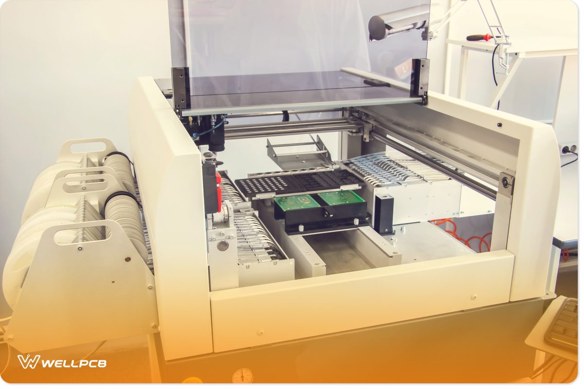
Automated soldering machine
Automated PCB assembly typically includes various processes, such as surface mount technology (SMT), through-hole technology (THT), and mixed technology.
- SMT: This widely used method involves directly mounting components onto the PCB surface using pick-and-place machines, with components placed on solder paste applied to PCB pads.
- THT: In this method, components are inserted through drilled holes in the PCB and soldered on the other side. THT is ideal for components needing mechanical strength or when surface mounting isn’t possible.
What Are the Key Components of Automated PCB Assembly Systems?
- Pick-and-place machines: These machines pick electronic components from reels or tubes and place them onto the PCB. Equipped with a vision system, they ensure accurate placement of components onto the solder paste applied to the PCB pads. Pick-and-place machines significantly speed up component placement compared to manual assembly.
- Reflow ovens: Reflow ovens help you solder electronic components onto the PCB surface. Once you place the components on the PCB, the assembly is put into reflow ovens to allow the melting of solder paste. As the solder paste melts, it sets electronic connections between PCB pads and components. Reflow ovens ensure a uniform soldering process with their controlled heating zones.
- Wave soldering machines: Wave soldering machines are essential for reliable and efficient soldering in through-hole technology component assembly. These machines allow PCB assembly to pass through a wave of molten solder. As a result, this wave wets the exposed leads, creating solder joints.
- AOI systems: After placing and soldering components, you can use automated optical inspection (AOI) systems to detect defects. Using image processing algorithms and cameras, the AOI systems compare the working PCB assembly with the expected assembly, detecting defects such as misaligned components, missing components or any soldering defects. AOI systems allow early detection of defects, allowing timely corrections.
A Step-by-Step of Automated PCB Assembly Process
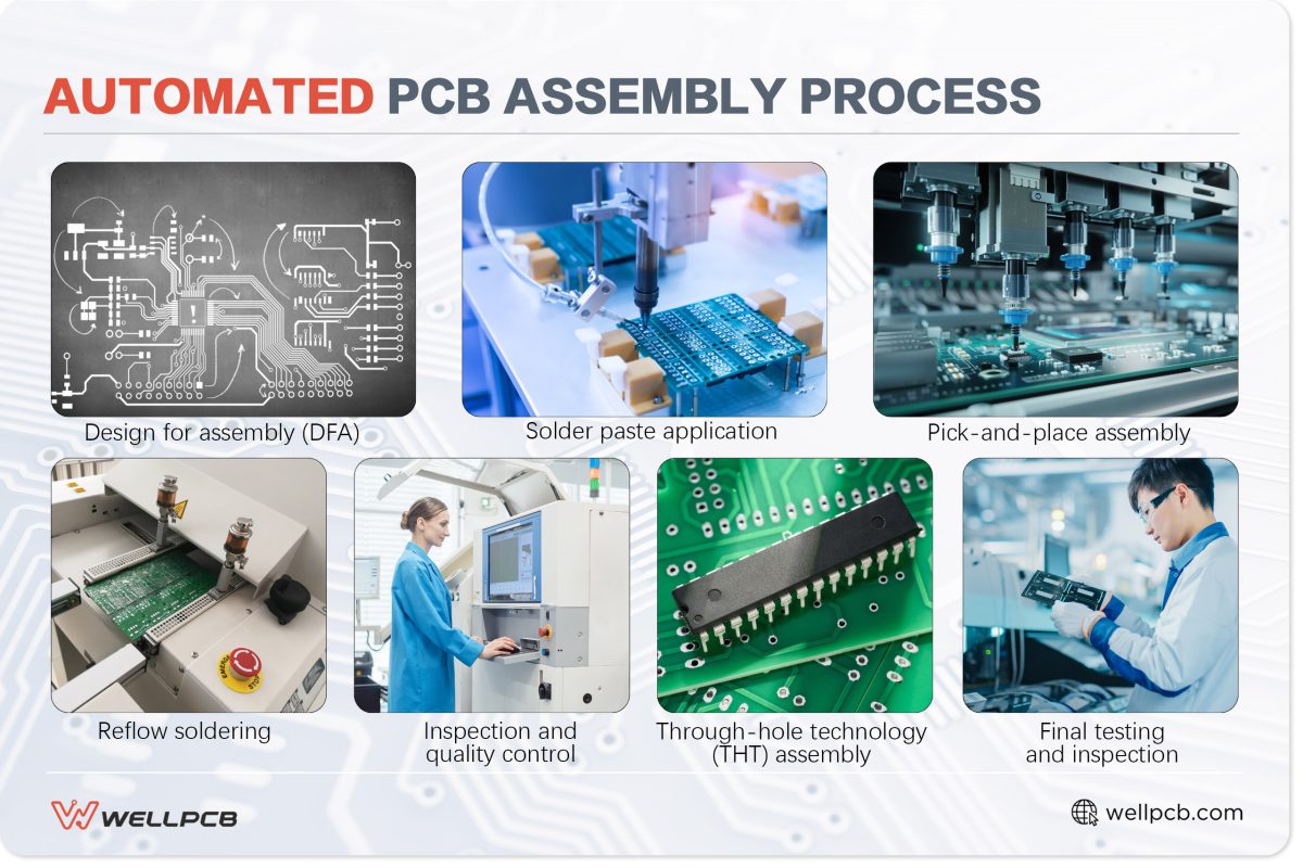
Automated PCB Assembly Process
Step 1: Design for assembly (DFA)
Firstly, you need to create a PCB layout in consideration of the automated assembly process.
While designing, consider component placement, their orientation, soldering accessibility and inspection.
You can use various CAD software tools such as Altium Designer, KiCad, and Eagle for this purpose.
The software features allow simulation of the assembly process so that you can identify any potential issues and optimize assembly accordingly.
Step 2: Solder paste application
In this step, technicians apply solder paste onto the PCB via stencil using a solder paste printer. Stencils, made of stainless steel, have apertures of the PCB pad size so that there is accurate deposition of solder paste on the PCB.
The technicians get to know the solder paste pattern on the PCB pads through the stencils only.
Make sure to pick the proper setup and design of stencils to avoid issues like excessive or insufficient solder paste, misaligned deposits or bridging between pads and ensure efficient and reliable solder paste application.
Step 3: Pick-and-place assembly
The step involves the automated placement of components onto the PCB pads, guided by the pick-and-place machine’s vision system.
These typically include surface mount devices, resistors, ICs, capacitors, and various other small components.
This critical process requires precision and accuracy to ensure the PCB design is followed correctly.
Step 4: Reflow soldering
This step involves passing the PCB assembly through a reflow oven to melt the solder paste and set a reliable joint between the pads and components.
Technicians can set the oven to different heating profiles—such as cool-down, ramp-up, and reflow—based on component requirements and solder paste conditions.
Step 5: Inspection and quality control
Next, verify component placement, solder joint quality, and PCB integrity using AOI systems. X-ray and visual inspections can also help identify defects that are difficult to spot with the naked eye.
While AOI provides comprehensive analysis through software and cameras, X-ray inspections reveal internal defects, while visual inspections catch external issues.
These inspections are essential to ensure compliance with various IPC standards and to meet customer specifications.
Based on the inspection results, technicians can take corrective action.
Step 6: Through-hole technology (THT) assembly
The THT assembly process involves inserting components with leads through PCB holes.
Wave soldering then secures these components to the PCB, ensuring high mechanical strength.
THT assembly is ideal when components require high current-carrying capacity or when surface mounting is impractical due to the shape, size, or specific application requirements.
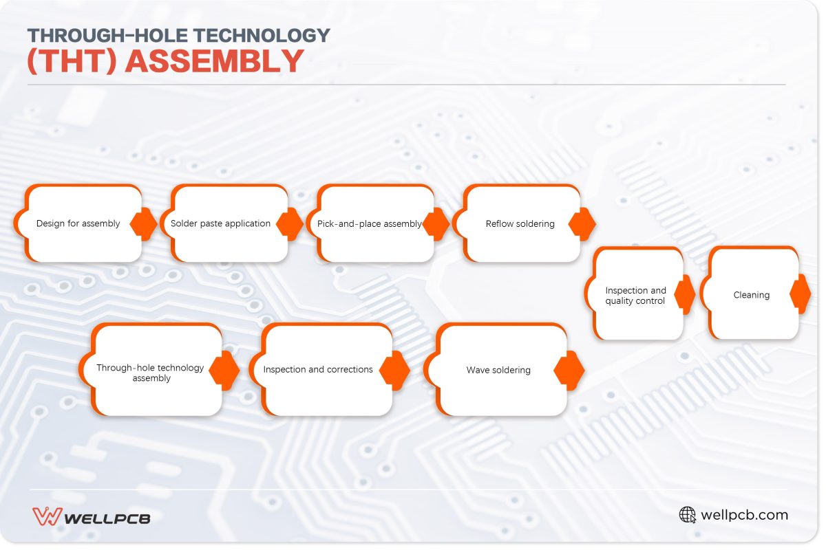
Through-hole technology (THT) assembly
Step 7: Final testing and inspection
The final testing verifies the functional performance of the assembled PCBs, ensuring they meet customers’ defined specifications. Several tests are performed in this stage:
- In-circuit testing (ICT): Using custom test fixtures or automated test equipment, ICT verifies component values and electrical connectivity.
- Functional testing: This test evaluates the overall functionality of the PCB, ensuring it works as intended in its final application.
Benefits of Automated PCB Assembly
Increased efficiency
Automation significantly increases the speed of the assembly process, which is otherwise performed manually.
By minimizing human error in soldering and component placement, automation ensures each PCB is assembled quickly and consistently according to the programmed instructions.
This leads to uniform quality across all PCBs.
Enhanced quality
Automated machines are consistently precise and accurate when placing and soldering components, ensuring customer requirements and design specifications are met.
AOI inspection also ensures that errors and inconsistencies are detected and minimized as early as possible.
By reducing the likelihood of errors, automated PCB assembly improves the overall reliability of the product.
Scalability and flexibility
Automated assembly lines enable the rapid production of high volumes without compromising on product quality.
Automation also provides flexibility in PCB manufacturing, accommodating different components like SMDs and THTs, as well as a wider variety of PCB designs.
Cost savings
Automated PCB assembly offers significant cost savings by reducing the need for manual labor, especially across PCB handling and assembling.
As the machines become more efficient over time, automation means lower cycle times, better resource utilization, and less scrap.
This is especially cost-effective in high-production scenarios, where manufacturers can maximize output while minimizing per-unit cost.
Industry Innovations and Trends in Automated PCB Assembly
The field of PCB assembly has seen some remarkable technological advancements lately, driving innovation and efficiency across the industry.
- Technically advanced pick-and-place machines are a prime example, leading to higher placement speeds, improved accuracy, and increased ability for PCBs to handle a variety of components.
- Intelligent soldering machines are another technological innovation defining the PCB assembly process. These connected leverage jetting systems place solder paste on the PCB pads precisely, quickly, and at scale.
- AOI systems are also increasingly sophisticated, with advanced algorithms and high-resolution cameras becoming more commonplace. These systems can detect even the tiniest defect, ensuring the highest level of accuracy, and use 3D inspection tools for more detailed evaluation when needed.
These systems will continue to deliver more safety and flexibility across the PCB assembly process.
Future Trends to Watch
Several emerging trends are also poised to shape the future of automated PCB assembly.
One of the most transformative of these trends is the integration of AI and machine learning algorithms into assembly line control systems.
These algorithms enhance quality control, optimize production processes, and detect failures—significantly improving overall efficiency.
Robotics is also set to take PCB assembly into innovative new territories.
As robotics technology advances, devices will handle increasingly complex tasks and production processes.
The future of PCB manufacturing is becoming increasingly smart and intelligent, thanks to the integration of IoT devices and sensors in production lines.
These sensors enable real-time monitoring of critical factors, such as weather conditions, product quality, and equipment performance.
With access to real-time data, manufacturers can implement proactive maintenance strategies, enhancing agility and reducing downtime.
Lastly, as sustainable and environmentally friendly practices are adopted across industries, automated PCB assembly technology will also become more eco-friendly.
From energy efficiency processes to reducing waste generation or recycling materials, such sustainable practices are guaranteed to revolutionize the electronics manufacturing industry.
Choosing the Right PCB Assembly Partner
- Expertise and experience: Always look for a partner with extensive experience in PCB assembly and a proven track record delivering quality output. It’s also helpful to ask if they have experience in projects and industries similar to yours.
- Technological capabilities: Your ideal partner will use highly advanced and automated equipment for soldering, pick-and-place, and inspection processes.
- Quality control standards: Always verify your PCB assembly partner’s certifications and quality control measures, such as their ISO certifications. Make sure their inspection processes are robust to ensure they can maintain high-quality standards across the production timeline.
- Flexibility and scalability: Your chosen PCB assembly partner should be able to handle varying production volumes. Similarly, they need to be flexible enough to accommodate any changes in requirements or production schedules.
- Communication and support: Always ensure your prospective partner has clear and reliable communication channels to share project updates and feedback.
Why Choose Us?
If you’re looking for a reliable PCB assembly partner with extensive experience, WellPCB is your ideal choice. Here’s why:
- We operate two PCB assembly facilities in Shijiazhuang and Shenzhen.
- With years of experience, we have successfully delivered projects across a wide range of industries.
- Our state-of-the-art facilities are equipped with highly advanced automated equipment.
- We adhere to stringent quality control standards and conduct advanced inspection processes, including AOI systems.
- We offer custom solutions that can cater to your exact needs and specifications.
- Our unwavering commitment to quality, innovation, and customer satisfaction sets us apart from the competition.
- With exceptionally fast turnaround times, we take pride in delivering projects quickly without compromising on quality.
- All our products meet REACH, RoHS, IPC, and UL standards, ensuring safety and reliability.
Contact us today for a quote or a consultation.
Get Started with Automated PCB Assembly
Automated PCB assembly enhances quality, increases efficiency, lowers costs, and enables scalability and flexibility, resulting in superior products that are more reliable for longer.
However, every step of the process—from picking the design and applying solder paste to placing components, melting solder paste, and utilizing AOI systems—must be monitored closely.
At WellPCB, we adhere to stringent quality control measures and standards to ensure our products meet the highest standards of performance and reliability.
Contact us today for all your electronics manufacturing needs and experience the difference in service and quality.


