Contents
- 1 What are Embedded Components
- 2 How to Design a PCB Assembly for an Embedded System
- 3 The Assembly Process for Component Embedded Printed Circuit Boards
- 4 Assembly Procedure for Embedded Components in PCB
- 5 Factors that Influence Embedded PCB Design
- 6 Advantages of an Embedded PCB
- 7 Challenges in Embedded System Design
- 8 Rounding Up
What are Embedded Components
Before we jump into what embedded components are, let’s brush up on the concept of embedded systems. The main idea behind embedded systems is to reduce the size of circuit boards while maintaining high integrity and performance.
Furthermore, embedded PCBs are circuit boards with components buried in their layers. Also, these embedded components help to enhance the performance of embedded systems.
There are many ways you can use embedded components. And the way you use them influences their manufacturing process. Initially, PCB fabrication and component placement were two concepts that required manufacturers to handle separately.
Now, the processes are not so distinct. Hence, you can design and manufacture boards with embedded components. Moreover, there are two ways to add embedded components.
- First, you can create open cavities to place embedded components. As a result, the components will remain visible on your final product.
- Second, embed the components into an internal layer. Consequently, the circuits will stay hidden.
Let’s take a closer look at the types of embedded components.
Note: Embedded components usually have two categories–Active devices and passive devices.
Embedded Resistors
Embedded resistors are passive devices that can enhance electronic performance. Also, the component moves individual devices from your PCB’s surface. Hence, it provides more surface space for other components.
However, embedded resistors must have specific tolerance and power ratings. Otherwise, it’ll burn or fail. Additionally, these devices don’t need solder joints or SMT vias, which increases PCB reliability and signal routing.
Embedded Inductor
An embedded inductor is a component that stores and supplies energy while balancing a circuit’s current flow. A standard inductor is quite complex to make, so you must embed them to save PCB surface space.
Embedded Capacitor
Embedded capacitors are a bit different because they use copper-clad laminates. However, these laminates eliminate the need to add decoupling capacitors on a PCB.
Embedded capacitors are thin dielectric materials positioned between two copper layers. Also, they act as decoupling capacitors due to their high capacitive density.
How to Design a PCB Assembly for an Embedded System
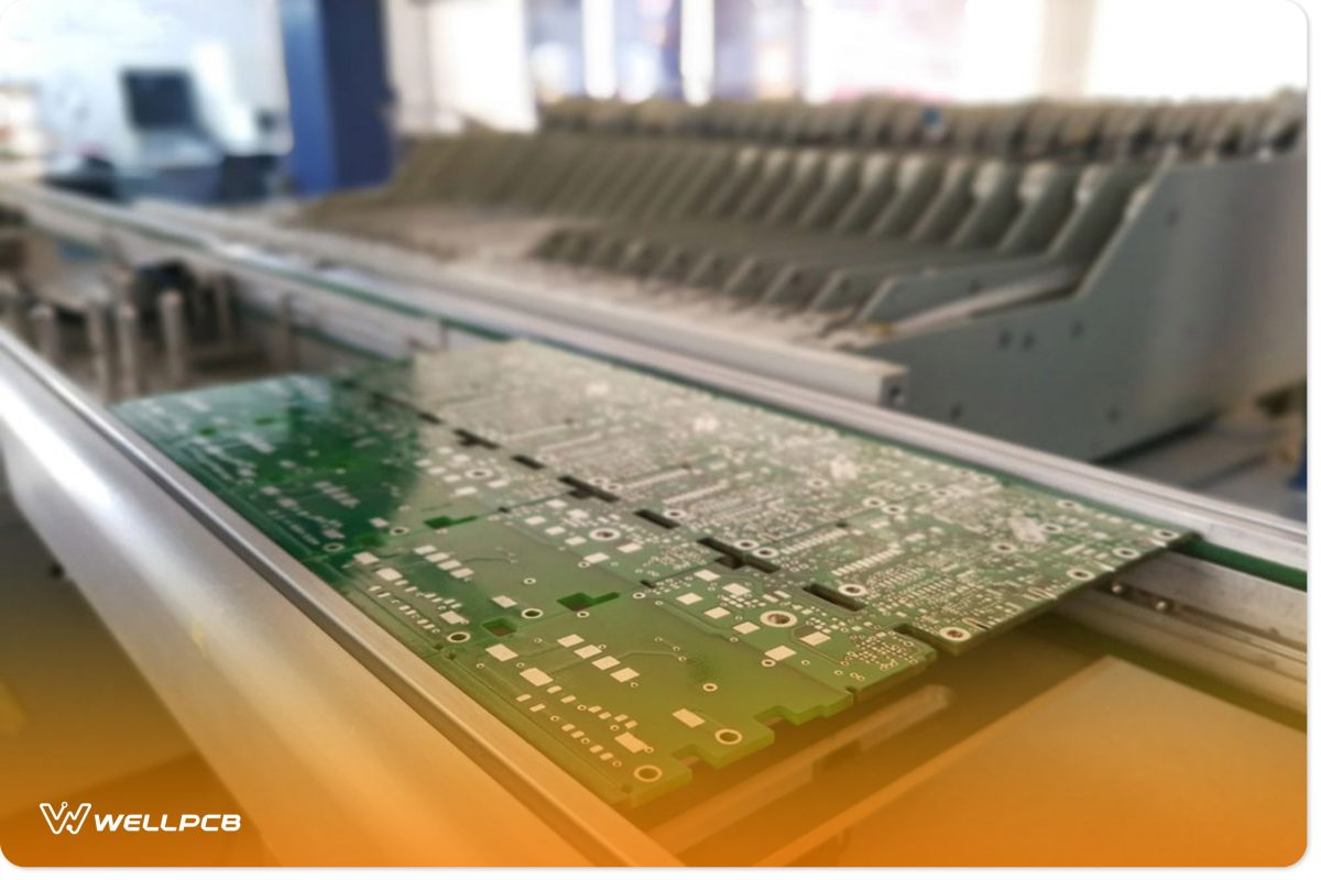
PCB Assembly
It can be tricky to design PCBs for embedded systems. But here are some tips to help you build a great embedded PCB design.
Define your Requirements
One of the major questions is: what do you want to achieve with your PCB? With this, you’ll know the necessary requirements.
Also, it’s crucial to consider how your PCB will interact with other areas of the embedded system and its size. These two factors will influence how complex your PCB will be during assembly.
Build your Schematic
After getting your requirements set, you’ll need to translate them into specifications for your schematic. Building a schematic includes choosing a suitable microcontroller and other components for the board.
Then, you can create a diagram showing where the manufacturers need to place them.
Microcontrollers are crucial for embedded systems. Hence, you must consider some factors before making a choice. These factors include the peripherals and processing speed.
Choosing the Right Automation Software
You’ll need the proper design automation software to place your schematic’s information. Then, the software will combine everything into a CAD file to instruct the assembling process of your PCB.
Selecting a Fabrication Method
The requirements you set earlier will determine the fabrication method your PCB needs. Some other factors that may influence the fabrication method are timeframe and budget.
Determine the Test-Type
Lastly, you need to select a test for your PCB. It’s crucial for the assembly process as it ensures your designs are standard.
Plus, manufacturers must test your design’s functionality before approval.
Note: You can choose different tests to ensure your designs meet the standard requirements.
The Assembly Process for Component Embedded Printed Circuit Boards
Using embedding technology for your components involves mounting. And there are two types you can use: Through-hole and Solder pad mounting types. Let’s take a closer look:
Through-Hole Mounting
Two processes are involved in a through-hole mounting method: Bare and chip mounting. For bare mounting, you’ll use conductive adhesive or plated through-hole options. Also, the chip mounting process offers similar options.
Solder Pad Mounting
Like through-hole mounting, solder pad involves bare and chip mounting processes. But that’s where the similarity ends. The bare method in solder pad mounting involves using flip-flop or wire mounting processes.
You must choose the process you want to use before embedding any components into your PCB. However, the chip mounting method involves adopting a conductive resin or wave soldering option.
Assembly Procedure for Embedded Components in PCB
Choosing a die bonding process is crucial when embedding bare die components. Also, you can apply other methods like ultrasonic wave bounding and ESC (Epoxy Encapsulated Solder Connection) if your components are mold packages, PDs, or WLCSP.
However, if you’re using AD mounting, it’s best to use solder with conductive resin or wave solder. The assembly procedure for embedded components with pads includes:
1. First, you need to know the different design and technology procedures before embedding. As a result, you’ll get active device feasibility and SMD embedding. While at it, you need to pay attention to your trace design.
2. Start fabricating the double-layered substrate before adding the solder paste coating if you’re working with a double-layered PCB.
3. Move to the wave soldering and IC assembly before mid-stack-ups and insulation filling. Lastly, do a hot press at the top layer stack-up.
Assembling components in a cavity is where things get tricky. And it’s because you may face problems that can cause high solder voidage. However, you can use the following workflow to avoid such issues, especially during solder printing or vacuum wave soldering techniques:
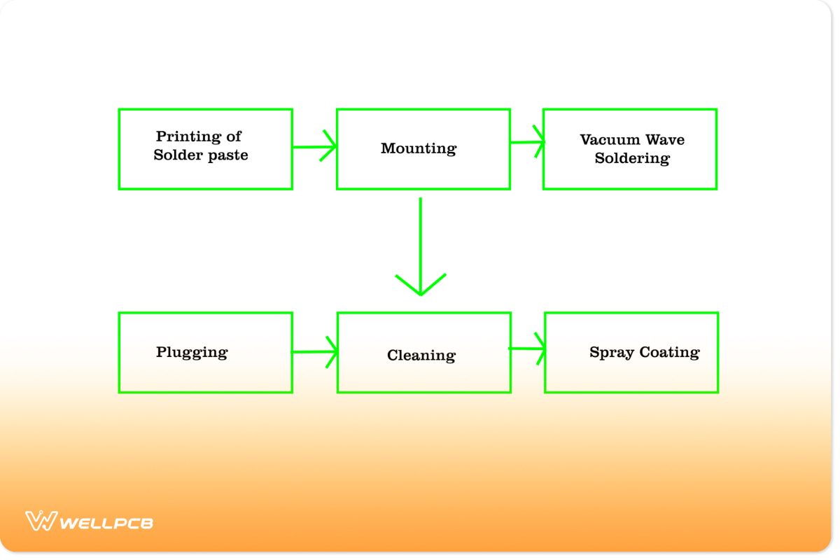
Workflow Process
Factors that Influence Embedded PCB Design
There are several factors you need to consider before building an embedding system. They include:
PCB Size
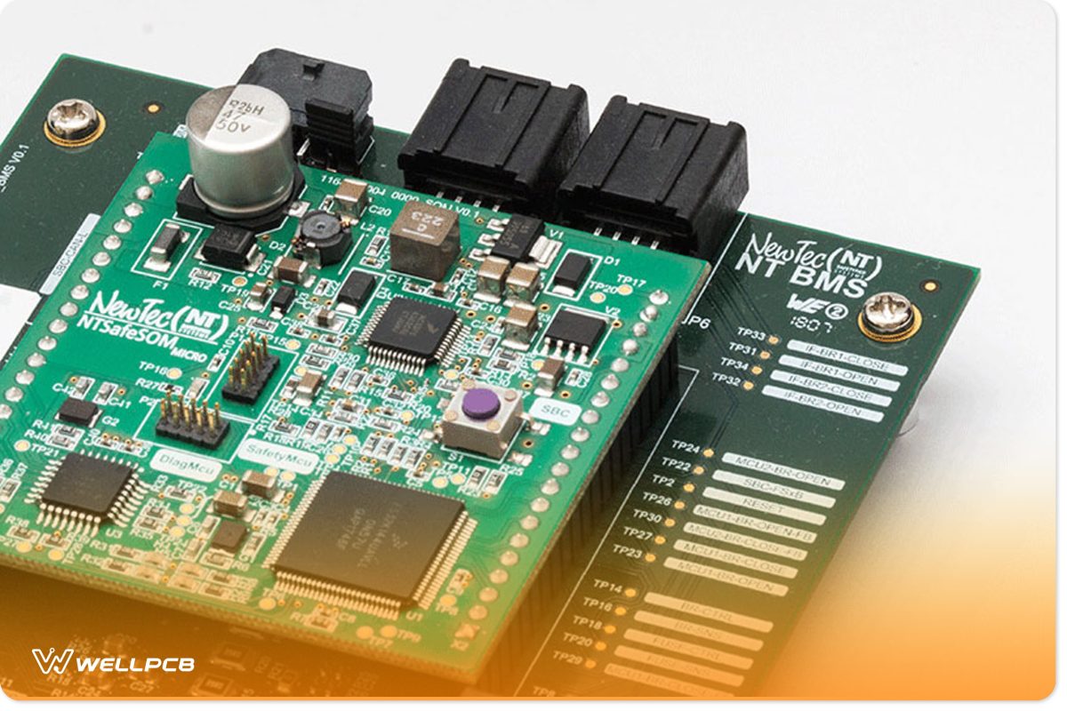
Small and Large PCB Size
PCB is a dominant factor that influences the structure of your designs. The size you choose must match the components you want to use. Also, selecting the proper size would allow correct placements and avoid overheating.
Thermal Management
If you’re working with high-current applications, there will be overheating issues. But you can increase your board’s thermal dissipation by increasing trace thickness or creating copper planes.
Component Placement
Board with Well-placed Components
Every PCB design requires some component placement rules. So, for embedded PCBs, it’s best to avoid placing heavier components close to the edge. Instead, such components should be on the PCB sides.
Also, you shouldn’t cluster power devices in one area. Instead, distribute them evenly on your board to get better thermal dissipation.
Advantages of an Embedded PCB
Here are some benefits you can enjoy from an embedded PCB:
Enhanced Heat Dissipation
Embedded systems have excellent heat dissipation capabilities and can prevent overheating problems.
It Is Cheap
Embedded PCBs are cost-effective. And it’s because the device has a single-chip compact design.
Strict Design Parameters
Embedded PCBs have pre-defined parameters. However, you can make some tweaks and adjustments to fit your design. But you can only do this in the form of extensions and additions.
Challenges in Embedded System Design
You must pay close attention to every design stage of an embedded system. Otherwise, you’ll face some challenges. While you can quickly fix your designs before manufacturing, any defects afterward may result in some expensive reworks.
Here are some challenges you may face with an embedded system:
- No surface space for other components
- Hardware testing challenges
- Packaging and integration challenges
- EMI emission
- Overheating
- High power consumption
- Inability to maintain validity
Rounding Up
Embedded PCBs are so versatile that you can use them in various applications. For example, you can use them in the military, consumer electronics, and even aerospace applications.
These boards undoubtedly offer incredible features that make them capable of dishing out high performance and density despite their miniature size.
Plus, it features embedded components that save some surface space for more complex designs and systems.
Although there are some challenges, you can easily avoid them by carefully designing your PCB and ensuring everything is correct before sending it for manufacturing.
Be sure to contact us if you want to manufacture an embedded PCB. We’ll be happy to offer the best PCB service.
