
Contents
- 1 Understanding PCB Assembly Quality Control
- 2 Key Quality Control Methods in PCB Assembly
- 3 Our Commitment to PCB Assembly Quality Control
- 4 3 Steps for Ensuring Effective Quality Control in PCB Assembly
- 5 Industry Trends and Updates in PCB Assembly Quality Control
- 6 Get Started With Our PCB Assembly Services
Understanding PCB Assembly Quality Control
Let’s examine some context around quality control processes during PCB assembly services.
What Is PCB Assembly Quality Control?
PCB assembly quality control is a set of processes in PCB manufacturing for inspecting, testing, and rubber-stamping all the assembly stages.
Quality control during assembly aims to ensure you receive all your PCBs on time with no defects.
Quality control guarantees that the final product is durable, can withstand different conditions, and performs optimally over time.
It also ensures that every batch of PCBs has undergone the same testing and is certified by qualified professionals.
Modern-day PCB assembly can be traced to the 1980s when surface-mount technology became popular.
The mass production of multilayer PCBs to support various industries required manufacturers to improve testing protocols to ensure reliability.
So, around the 1990s, new design testing and quality assurance guidelines emerged.
We can trace the emergence of microvias and flex-PCBs to these quality control guidelines.
Why Is Quality Control Crucial in PCB Assembly?
Quality control (QC) covers visual inspection, automated inspection, and checking for internal faults or defects.
Higher manufacturing quality control standards lead to optimal PCB performance and more reliable electronics.
These controls eliminate errors and reduce the margin for malfunction during usage.
Since manufacturers implement these measures for entire production runs, PCB batches are consistent in quality with no mistakes occurring externally and beyond the surface.
Qualified professionals use dedicated machines to inspect every board so it’s delivered error-free.
Manufacturers and designers use updated QC systems to provide people with functional, reliable, and safe PCBs for their projects.
Under these systems, end-users avoid taking on unnecessary repair or reworking costs associated with defective boards.
Key Quality Control Methods in PCB Assembly
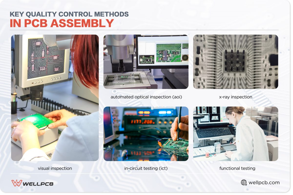
Here are five essential PCB testing methods that PCB manufacturers factor into their quality control processes during assembly.
1. Visual Inspection
During visual inspection, inspectors use specific tools and techniques to check for surface and underlying defects. We’ve detailed these in the table below.
| Stage | What Happens | What Is Checked |
| Initial inspection | Inspectors check the PCB using design documents as a reference. | Design dimensions, PCB layouts, and correct component placement |
| Component inspection | Inspectors check all components for correct board placement. | Correct placement for resistors, capacitors, and all other core components Correct polarity for full electrical functionality (LED and diodes are checked at this stage) |
| Inspecting the soldering | Inspectors examine the quality and finishing of the solder joints. | Solder joints are smooth and wetted Solder bridges have no misplaced connections between pads No cold solder joints (poorly connected solder joints are dull and grainy) Solder is enough to form strong joints |
| Final check | Quality control auditors check for any visible defects. | Labels and markings are visible, correct, and readable. No scratches, cracks, or visible physical defects. No residue or contaminants. |
Tools and Techniques Used in Visual Testing
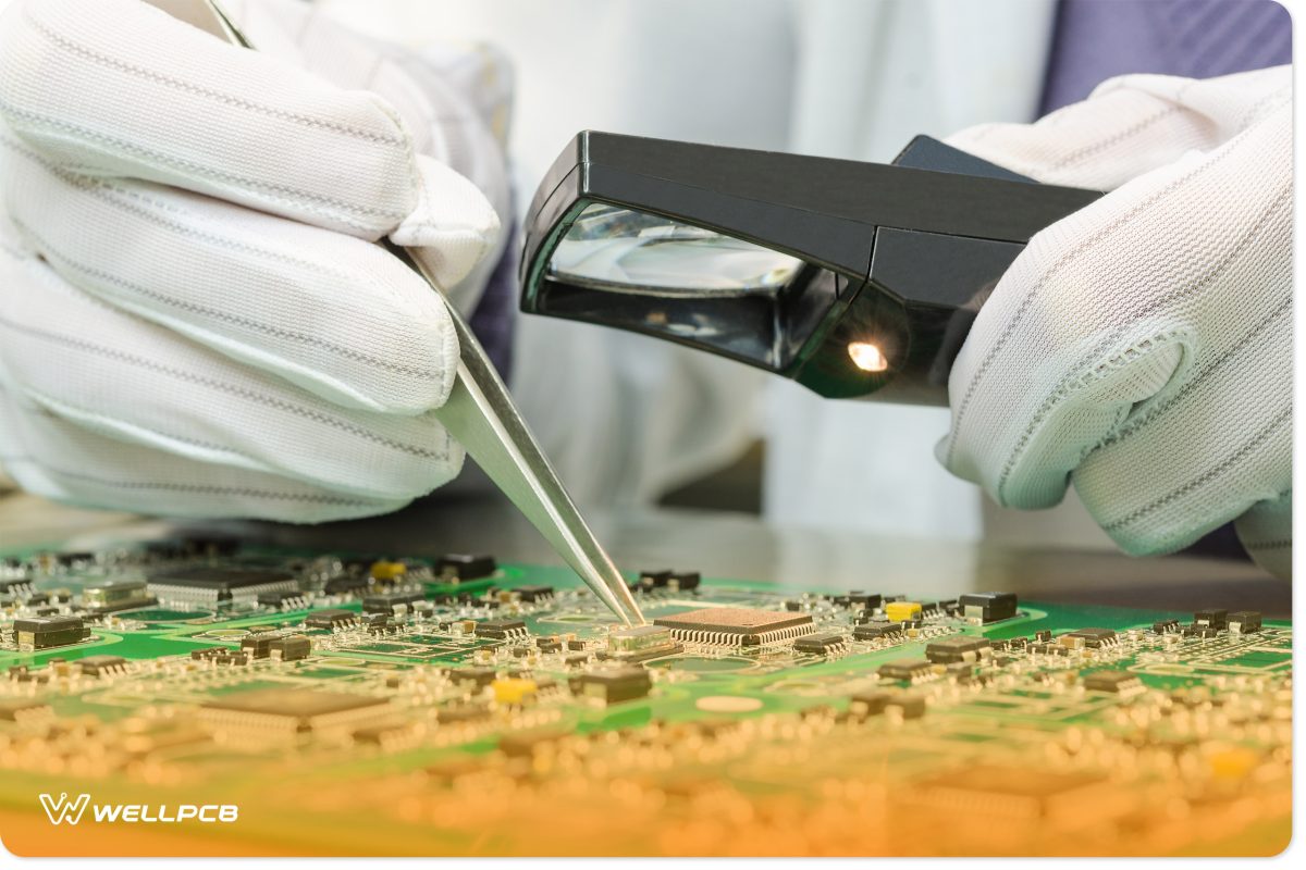
High-precision magnifying devices and microscopes are vital for identifying tiny defects on boards during manufacturing. When additional visibility is required, inspectors use digital magnifiers to check errors.
Light-adjustable inspection stations enhance defect detection by providing extra light during visual inspection. Light-aided inspection is especially useful during coating checks, as it helps verify that the coatings have no pricks or tears. Also, it helps confirm that coatings are even and have attained the correct thickness in only the relevant coating sites.
Inspectors use 2D and 3D cameras to provide full-cover view of the PCBs. 2D cameras check for cracks and missing components, while 3D cameras check for soldering mishaps and correct component alignment.
Defects Identified Through Visual Inspection
Some common defects you can identify at this point of PCB quality control include:
- Soldering defects (rough solder joints, misconnected solder bridges, excess/insufficient solder)
- Misaligned or missing components
- Cracks
- Scratches
- Lifted leads
2. Automated Optical Inspection (AOI)
Automated optical inspection uses imaging tools and software to check defects in PCBs. It’s a fully non-contact method that gives a complete, accurate analysis of beneath-the-surface defects.
How AOI works
- A computer is pre-loaded with an image of a good printed circuit board that has passed quality control checks as a reference.
- The PCB to be inspected is fed into the AOI machine.
- Advanced cameras take well-lit pictures of the PCB from various angles.
- The AOI system lines up all the pictures and presents a full view of the PCB.
- Then, it analyzes the circuit board with images of the good PCB to highlight differences that can be identified as discrepancies.
- Defects are grouped into levels of severity.
- Adjustments are made on the defective PCB.
- A QC auditor can re-inspect repairs before a final AOI check.
Using AOI early in the assembly process cuts production time spent redesigning and reworking defective boards, and having the systems in place allows for immediate correction before the boards move to the next stages.
Besides, it lowers production costs in repairing boards with cracks or inconsistencies. Because defective boards don’t progress through additional manufacturing steps, it also saves materials and reduces waste.
Finally, AOI improves production turnaround time as defects are detected and addressed incrementally, optimizing throughput for each batch of boards.
3. X-Ray Inspection
X-ray inspection detects defects hidden under the surface and between layers. If left unaddressed, hidden defects can reduce PCB functionality, reliability, and durability. In worst-case scenarios, they can even harm end users.
X-ray inspection works best when dealing with miniature PCB components, hidden solder joints, and multilayer designs common in high-tech electronics.
Equipment and Techniques Used in X-Ray Inspection
X-ray systems are either automated 2D or 3D systems.
2D systems check single- or double-layer PCBs where imaging from the top and bottom sides is required. 2D X-ray techniques, such as topography, give a view of both sides of the board, but they are limited.
The image quality lacks depth, therefore compromising the quality control outcomes.
3D systems use computed tomography (CT) and laminography to create 3D images that provide an in-depth look at the PCB.
The PCB images are then deconstructed into cross-sections to view possible internal errors, and image processing software such as Phoenix Xact renders high-resolution images to examine.
As a result, the inspector has a better view of separate layers to give a detailed assessment of inner defects.
Defects Identified Through X-Ray Inspection
Some common defects you can pinpoint during X-ray PCB inspection include:
- Solder joint defects such as shorts, bridges, and voids
- Ball grid array defects such as uneven ball sizes, misaligned solder balls, and missing solder balls
- Chip scales package defects such as cracks and fractures
- Component placement defects
- Plated through-hole defects such as inadequate fill and poor plating
4. In-Circuit Testing (ICT)
In-circuit testing (ICT) is fast and accurate in checking component defects and circuit continuity. It takes about two minutes or less per assembly, making it invaluable in mass assembly.
ICT is applied in both when the PCB has power and when the power is off. During this process, the manufacturer ensures all of the following areas are functional:
- Component marking and spacing
- Open circuits
- Soldering
- Resistor, capacitance, and inductance values
- Jumpers and switches
Overall, ICT ensures the board has working circuits and components during assembly before moving to final testing.
The Process of In-Circuit Testing
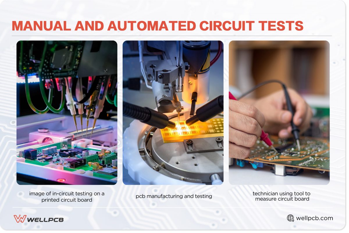
Accurate ICT systems have a custom test fixture to hold the PCB and ensure electrical contact with the board’s test points. Additionally, a test program controls the system and outlines the tests for each component.
A qualified inspector mounts the PCB on the test fixture and aligns it with the probes. The inspector then connects the ICT system to perform the tests. From there, the system applies signals to all the components and records the output. Finally, the inspector collects all the data for analysis and to identify component anomalies while checking against the PCB designs.
Common Issues Identified Through ICT
- Incorrect component values
- Poor soldering that could affect the circuitry
- Poor circuit connections
- Component shorts
- Missing components
5. Functional Testing
Functional testing certifies that the printed circuit board works as designed and is ready for use in various applications and electronic devices.
Types of Functional Tests Performed
| Test | Process | Why It Is Performed |
| Power-on self-test | Apply power to the PCB. | Check if the PCB powers up Check voltage, consumption, and component functionality |
| Boundary scan testing | Apply the IEEE 1149.1 JTAG process on pins’ integrated circuits. | Check open circuits and identify connection issues |
| Functional verification testing | Apply electrical signals to simulate an operational environment. | Check if the PCB powers upCheck voltage, consumption, and component functionality. |
| Environmental stress test | Test the PCB in different environments. | Check how the PCB performs under various real-world conditions such as shock, vibration, high EMI, and humidity |
| Load tests | Apply various loads to the PCB and note peak demands. | Check how the PCB performs under various real-world conditions such as shock, vibration, high EMI, and humidity. |
| Signal integrity test | Inspectors use probes, vector network analyzers, and signal generators. The record graphs show the signal output for each device. | Evaluate how the PCB functions under different load stresses without failure or damage. |
| Communication interface test | Peripheral devices are fed into the PCB communication interfaces such as Ethernet or USB ports. | Ensure data transmission and overall interface function |
| Firmware/Software test | Firmware/Software is loaded, and the PCB is tested using various programs. | Check if the PCB performs with its intended software/firmware |
| Safety and compliance | Inspectors test the PCBs according to their required compliance standards. | Determine that the PCBs pass regional and global organizations’ safety and compliance guidelines. |
| End-line testing | Safety and Compliance | Ensure the PCB matches the customer’s requirements and is ready to be delivered |
Benefits of Functional Testing for End-Users
Functional testing gives end-users fully functional, reliable printed circuit boards that pose no risks. After passing these tests, the PCBs meet safety and environmental quality standards as per industry regulations. That way, end-users are assured the electronic devices they use are high-quality.
Our Commitment to PCB Assembly Quality Control
WellPCB is committed to producing high-quality, reliable printed circuit boards, and our PCBs undergo rigorous testing during the assembly process.
Our Quality Control Measures
Our factories have a team of certified inspectors who review all PCBs during and after production. The internal QC auditors run final checks on individual products before shipping.
Not only do they follow operational procedures, but we also have a 98% positive evaluation and satisfaction score before shipping out your products.
To remain compliant, we continually train our professionals to follow the most up-to-date industry standards. We are UL, ISO14001:2015, ISO9001:2015, and IATF16949: 2016 certified. Furthermore, all our products must meet IPC and ROHS standards to be qualified for international markets.
Proprietary Techniques and Technologies
We don’t begin quality assurance at the end of production. Our modern, automated equipment imported from Germany, Japan, and Israel produces reliable PCBs right from the start.
We also have more than 200 qualified technicians and QC auditors with years of experience overseeing our human-run process. For example, our Shijiazhuang factory has five top-range 5 Siemens SMT lines that reduce the chances of misplaced or missing components. And our Shenzhen factory has well-serviced AOI and X-ray machines for quality control.
Benefits of Our Proprietary Techniques for Quality and Efficiency
We keep our machines well-maintained and our processes fast to give you durable PCBs in quick turnaround times. Whether your projects are medium-sized starter projects or large-scale productions, we always employ techniques that provide defect-free goods.
Furthermore, you make a commitment to environmental sustainability when using our RoHS-compliant materials.
3 Steps for Ensuring Effective Quality Control in PCB Assembly
Follow these steps for a streamlined PCB manufacturing process. You’ll reduce your costs and receive a high-quality product at the end of assembly.
1. Design for Quality
There are significant time and cost savings when you pay attention to quality while creating your printed circuit board layouts.
- Simplify designs for quick and efficient quality control. (Complex designs extend production and PCB inspection time, adding room for error.)
- Use standard components to ensure a thin margin for errors during assembly. This also makes reworking easier if there are faults.
- Build a prototype in the design phase to make production for bigger batches more efficient. Furthermore, running simulations exposes any potential quality control mishaps.
- Follow and review Gerber files, bill of materials, and centroid files, keeping detailed records of changes.
- Document the process from the design phase.
Software Tools and Resources To Assist in Design
As professional PCB manufacturers, we recommend the following tools to assist in designing your printed circuit boards.
- Eagle(Fusion360): Autodesk’s design tool lets designers view schematic designs and layouts, integrating with mechanical CAD. There’s also a community of designers who engage regularly. It’s best suited to intermediate and advanced designers.
- DipTrace: An easy-to-use PCB design tool for 3D modeling and creating libraries for references and follow-up.
- Siemens PADS PCB design software: Professional design tool for advanced users and complex PCB projects.
- Altium: A popular design tool among professionals for 3D visualization and an all-around design environment. It’s the most preferred for high-volume PCB production.
2. Follow Manufacturing Best Practices
At WellPCB, we’re well-versed in the entire PCB manufacturing process. Follow these best practices to get optimal results for your project:
- Clearly define design specifications, including materials, layering, and component placement.
- Hold updated reference files, including Gerber Files.
- Document procedures for each manufacturing job.
- Assign specific manufacturing quality inspectors for every project.
- Prioritize smooth workflow to cut down on errors and production delays.
- Work with verified suppliers to maintain manufacturing consistencies.
- Pay attention to customer feedback.
- Continuously train and upskill staff on incoming trends and industry changes.
3. Perform Regular Audits and Inspections
Regular audits on machines, procedures, and customer feedback ensure manufacturers keep updating systems to maintain reasonable production costs and reduce errors. Furthermore, audits help you preserve customer confidence in your products.
Here are our recommended tools and techniques for effective auditing:
- The 5 Whys technique: This is a root cause analysis (RCA) technique used to investigate why a specific problem exists. In quality inspection, it examines feedback, highlights recurring issues, and searches for answers until you can identify the key problem.
- Failure mode and effects analysis: A process analysis tool that identifies manufacturing errors and failures and examines their consequences on users.
- Proper documentation: Auditing requires a follow-up on every file that tracks the manufacturing process. It tracks costs, redesigns, reworks, changes, and successful delivery.
Industry Trends and Updates in PCB Assembly Quality Control
Sharpening your teams’ skillset and knowledge of industry standards boosts user confidence and reduces the manufacturer’s operational costs. Here’s what’s currently trending in the PCB manufacturing industry.
Recent Changes in Quality Control Methods
- Introduction of IPC 6012 Class 3/A assembly services: This is the highest class of PCBs that comes with newer quality assurance guidelines. It deals with hyper-complex PCBs that are standard in high-level applications, such as avionics.
- 3D AOI: AOI is evolving into automated systems. Additionally, manufacturers are keen on using automated 3D AOI to detect defects from more angles.
- AI and machine learning: Smart manufacturing integrates AI and ML into production to collect and analyze real-time data during assembly.
As the industry adopts these trends, manufacturers are cutting production times and providing customers with complex yet error-free PCBs.
Future Trends To Watch
- Big data analytics: Manufacturers are investing heavily in data analytics, especially for high-volume productions. As miniaturization becomes more normal, fast data analytics will likely play a massive role in improving quality standards.
- Predictive maintenance: This could be a future trend that anticipates failures to develop likely solutions that boost efficiency and PCB safety.
- Real-time monitoring: Manufacturers will start using real-time monitoring systems and data analytics for direct feedback and error correction, which can help reduce production time and improve quality control efficiency.
- Workplace development: As demand for more advanced technology rises, manufacturers must continue upskilling technicians and quality assurance inspectors through intensive training programs on incoming trends.
- Environmental consciousness: More global markets are demanding increasingly stringent controls on safety and quality while focusing on sustainability. For example, there’s a growing tendency to move towards lead-free soldering.
- Advanced testing methods: Manufacturers must invest in more advanced X-ray equipment and fully automated error-detection systems.
Get Started With Our PCB Assembly Services
Manufacturers implement various PCB inspection measures to ensure production is defect-free and reliable for end-users. During the production process, PCBs undergo a list of human and automated checks before release.
But top-quality PCB manufacturing is only one part of reliable PCB production. For safe, reliable and durable electronics, quality control must be strict and consistent.
At WellPCB, we regularly update our certifications and educate our production teams to adapt to industry changes.
We’re not only focused on producing PCBs but also committed to ensuring your products meet global safety standards.
Are you ready for reliable, high-quality PCB production in record time? Use our 24/7 communication lines to request a quote from our team.
We promise top-notch service and the best value products at affordable prices.


