
Contents
What is Surface Mount Technology (SMT)?
Before PCBs become complete printed circuit board assemblies (PCBA), they go through a mounting process where electronic components are permanently attached to the board. SMT simplifies this by enabling components to be mounted directly onto the PCB surface, without needing to drill any holes.
We refer to these surface-mountable component packages as surface-mount devices (SMD). The components designed for SMT are called surface-mount devices (SMDs), and their compact design allows for high levels of automation and precision. This has led to smaller, lighter, and more repeatable assemblies that encourage innovation in PCB design.
Thanks to SMT, the assembly process is easier, faster, and less strenuous for assembly line workers. This is because it primarily involves placing PCB components on the board. But when did we start using this technology? In the next section, we’ll share answers.
Brief History of SMT
SMT originated in the 1960s when it was referred to as “planar mounting.” It was pioneered by IBM, before being adopted by NASA for their Launch Vehicle Digital Computer.
Although introduced early, SMT didn’t gain widespread adoption outside government applications until 1976. By the mid-80s, SMT was being used in about 10% of PCBs.
Its popularity only grew from there, as it enabled greater functionality in smaller devices.
As such, handheld electronics such as digital cameras and camcorders were all made possible through SMT.
The 90s saw further SMT-driven advancements, including 3D, high-density, and micro-assemblies. Today, the use of SMT continues to expand. While the usage of THT declines 11% per year, SMT adoption grows by 8% each year.
While the terms “Surface Mount Technology” and “Surface Mount Devices” are closely related, they’re not the same—SMT refers to the technology and process, while SMD refers specifically to the components used in this process.
Key Terms Related to SMT
Some key phrases you may come across when dealing with SMT include:
- Surface mount equipment (SME): Machinery used to attach components to the circuit boards.
- Surface mount assembly (SMA): The complete SMT assembly process, covering everything from gathering and mounting the components, to verifying the quality of the PCB.
- Surface mount device (SMD): Components that use surface mount packages. Just like through-hole components, these can be electromechanical, active, or passive. These are also referred to as Surface Mount Components or Surface Mount Device Components.
- Surface mount packages (SMP): Packaging that enables components to be mounted. While often discussed in the context of integrated circuit systems, SMP can refer to the packaging of any surface-mount component (SMC).
SMT vs. Through-Hole Technology
The primary distinction between SMT and THT lies in how components are mounted on the PCB:
- SMT: Allows components to be placed directly on the PCB surface without drilled holes, enabling components to be mounted on both sides of the board. SMT components, often smaller and lead-free, have reduced parasitic capacitance and inductance, making them suitable for high-speed PCBs.
- THT: Requires drilled holes for component leads, which are then soldered from the other side, limiting mounting to one side of the PCB. While THT lacks automation efficiency and is used mainly for prototyping or small-batch productions, it provides stronger mechanical bonds. This stability makes THT ideal for high-stress environments, such as aerospace and military applications.
SMT enables large-scale automated assembly and allows for complex, multi-layer PCB designs, which are essential in modern electronics. However, THT’s strength and durability still make it valuable for certain specialized applications where robust connections are essential.
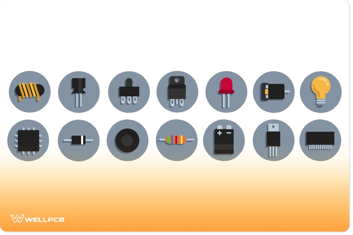
Types of Surface Mount Devices
SMD components can either be active or passive. This classification is based on factors such as their energy source, functionality, power gain, current flow, and whether they require an external power source.
Active Components
Active SMD components are capable of:
- Delivering power to the circuit
- Producing energy in the form of voltage or current
- Providing power gain
- Controlling current flow
These components also require an external power source to operate.
Examples of active SMD components include transistors, diodes, and integrated circuits. Let’s explain each in detail.
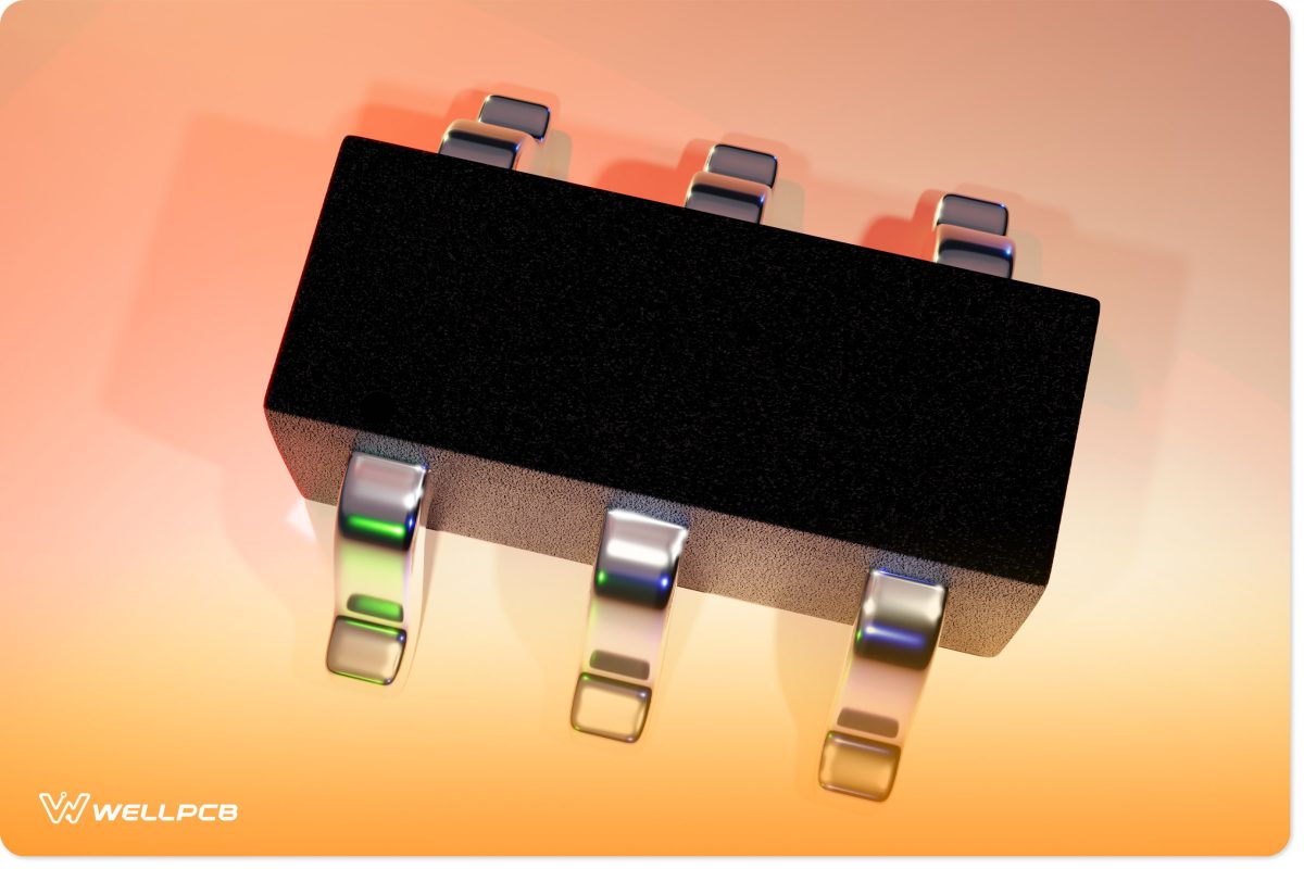
Transistors
As with THT transistors, SMD transistors have several purposes, including switching, signal modulation, oscillation, voltage regulation, and amplification. However, the most glaring difference between SMD and THT transistors is how they sit on the PCB. Whereas most THT transistors sit upright, SMD transistors typically lie flat. w they sit on the PCB. Whereas most THT transistors sit upright, SMD transistors typically lie flat.
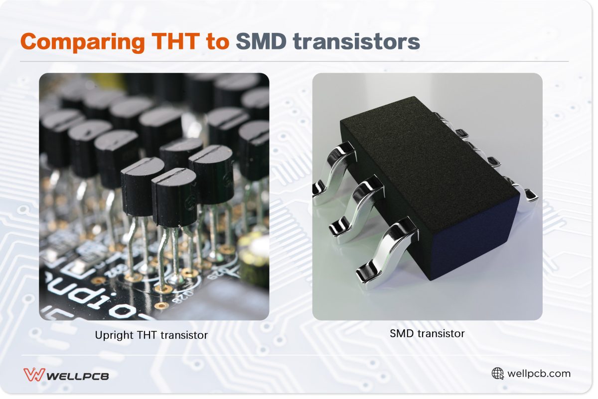
Small-outline transistors (SOT/SC) are the most common type of SMD transistors—especially the SOT-23 variation. Other package types include Dual Flat No-Lead (DFN), Quad Flat No-Lead (QFN), and Transistor Outline (TO).
Diodes
Diodes are dual-lead components that force a circuit’s current to flow in one direction, known as rectification, which ultimately converts AC to DC. Most SMD diodes come in rectangular packages, with leads extending from their widths. The three main SMD package types are:
- Small Outline Diode (SOD)
- SOD123
- SOD323
- Surface Mount Assembly (SMA)
- SMA
- SMB
- SMC
- Flat no-lead and power packages
- TO-220
- TO-252
- TO-263
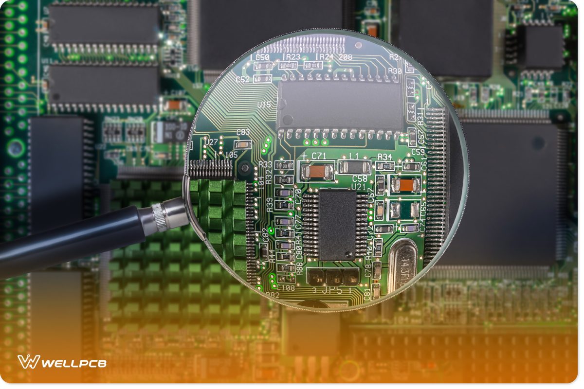
Integrated Circuits (ICs)
Integrated circuits (ICs) are essentially miniature packaged circuits. These are available in the following package types:
- Small Outline Integrated Circuit (SOIC)
- Small Outline Package (SOP)
- Thin Small Outline Package
- Think Shrink Small Outline Package
- Quad Flat Package (QFP)
- Ball Grid Array (BGA)
- Plastic Leaded Chip Carrier (PLCC)
SOT, DFN, and QFN IC packages are also available.
Passive Components
Passive SMD components are devices that:
- Use power or energy from the circuit
- Store energy in various forms, such as power or magnetic fields
- Do not provide power gain
- Do not alter or control the current flow
- Do not require an external source
Examples of passive components include capacitors, resistors, and inductors.
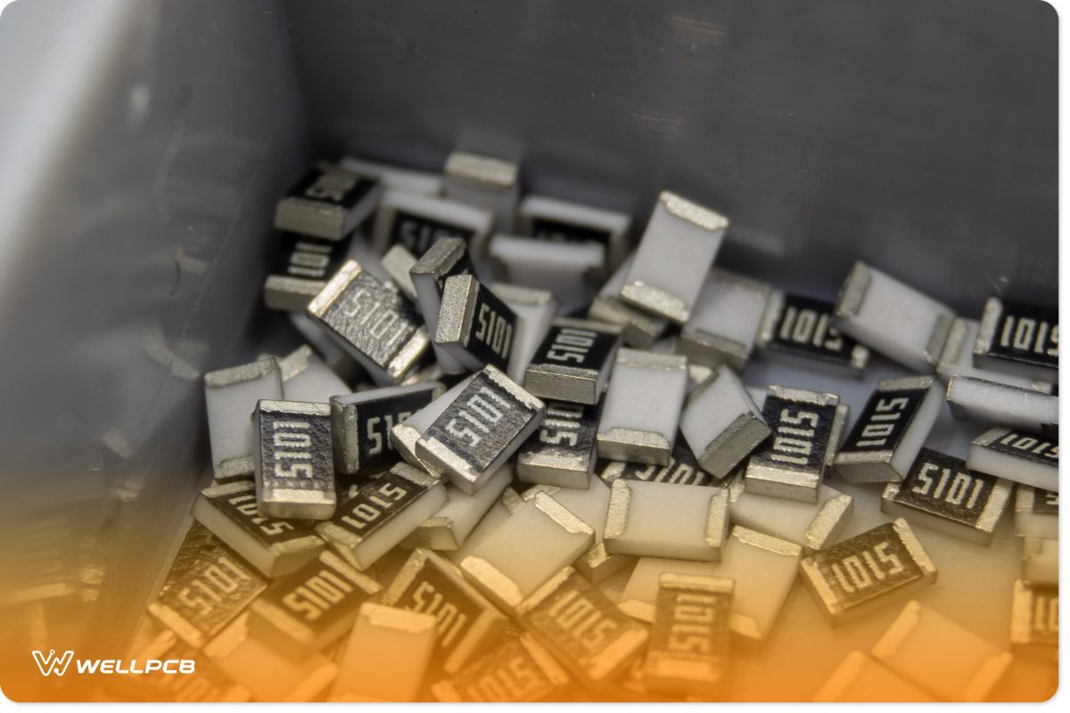
Resistors
SMD resistors fall into two main categories: chip (R) and network (RA/RN). Chip resistors are the most common.
Chip resistors display resistance values with printed codes, where the first digits indicate resistance, and the last digit is a multiplier. For instance, “105” is equivalent to “1M Ω”, while “672” is equivalent to “6.7K Ω”.
Network resistor chips feature high-grade ceramics with metal electrodes on either end. They each contain multiple resistors with similar properties, while their resistance values are coded similarly to chip resistors.
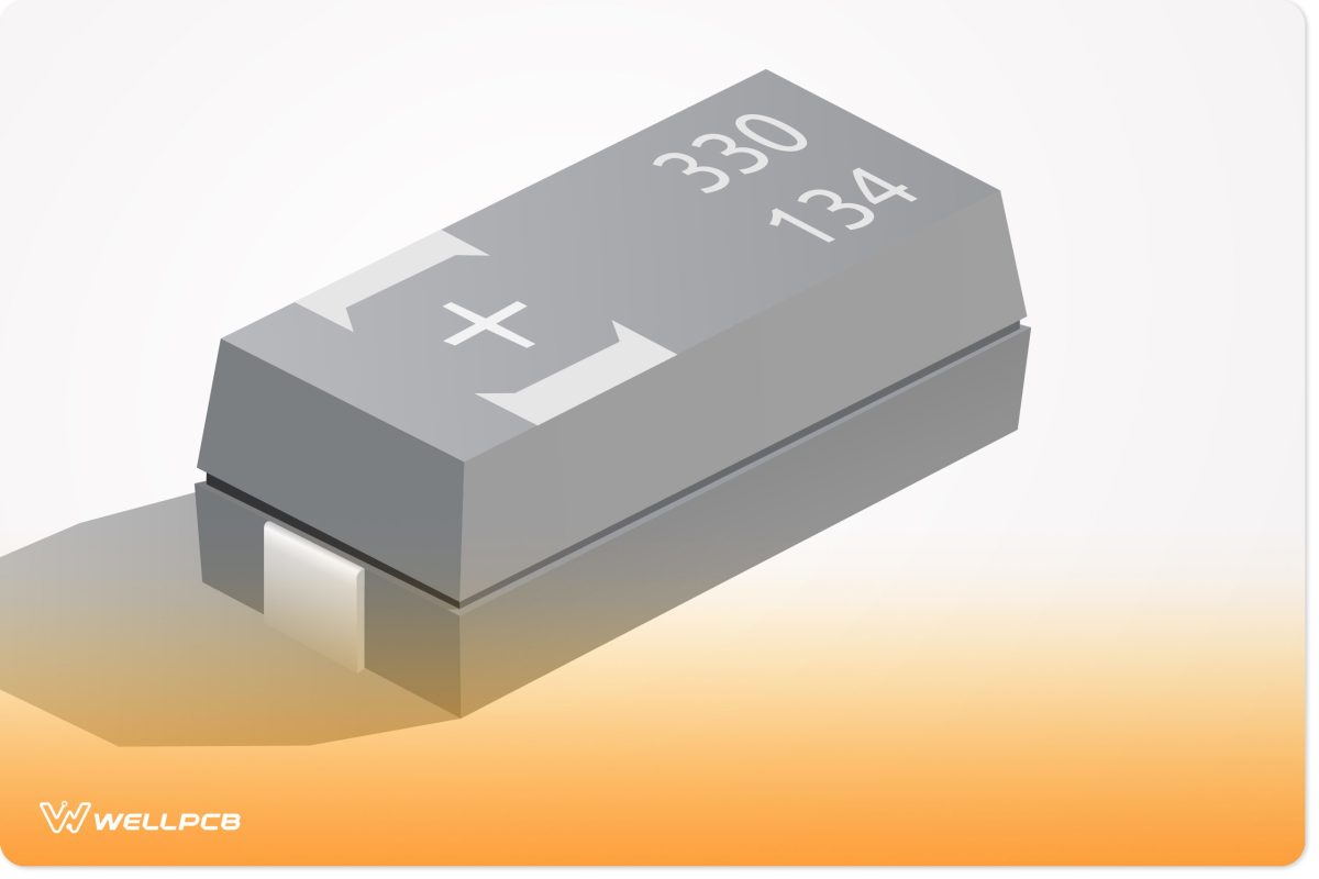
Capacitors
SMD capacitors are available in two varieties: ceramic and tantalum. Ceramic capacitors are constructed from interlocked ceramic dielectric blocks with metal electrodes coated in plated tin for stability. These capacitors are ideal for high-frequency applications and provide excellent reliability.
Tantalum SMD capacitors use tantalum as their anode material. As such, they offer high capacitance values in a compact package and are ideal for applications with limited space.
Inductors
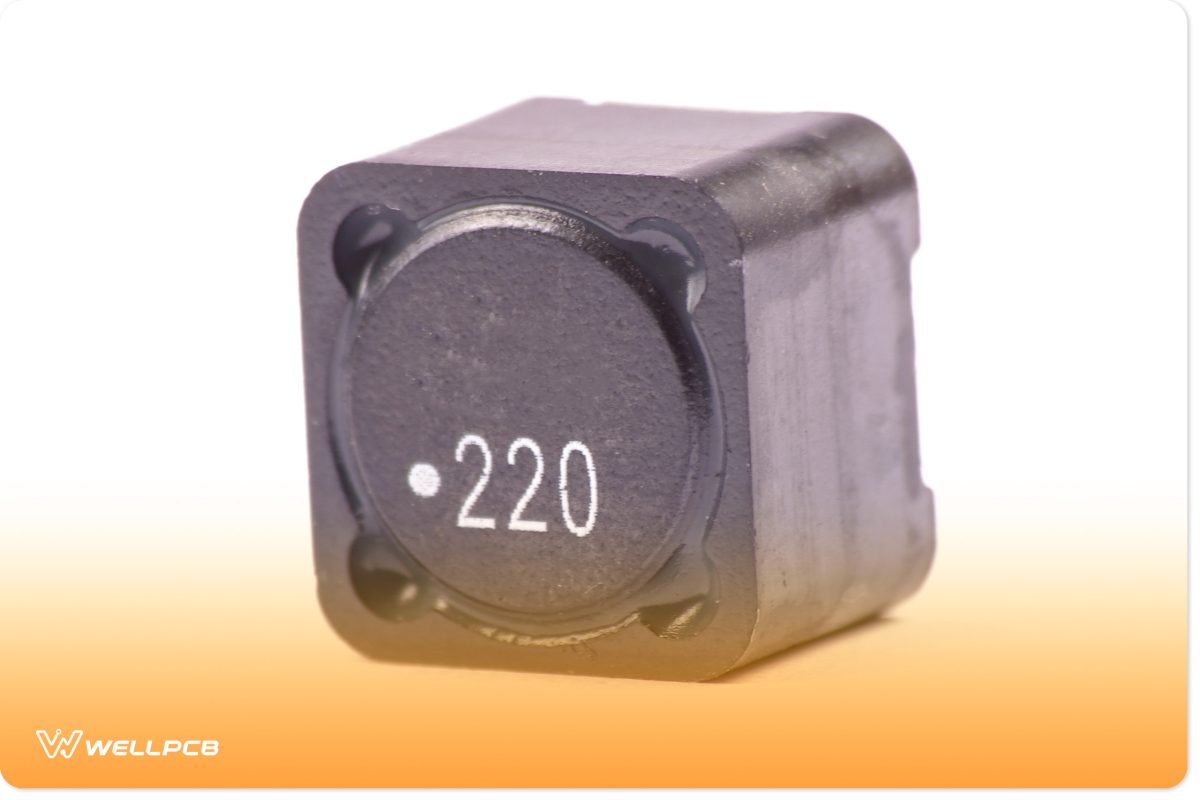
SMD inductors are available in three types:
- Multilayer chip inductors
- Wire-wound inductors
- Ferrite beads
SMD inductors come in various shapes and sizes. As with most components, indicator values are typically marked on the package in standard codes.
For example: “101” represents 100 µH, where the first two digits are the value and the last is the multiplier (10 x 10^1).
Other Common SMD Components
Other notable SMD components include:
- Light emitting diodes (LEDs): SMD LEDs contain a semiconductor crystal that emits light when current passes through. They are available in various sizes and can be identified by their package markings, which also indicate polarity.
- Transformers: SMD transformers are designed with surface-mount headers for easy PCB integration and consist of a wire-wrapped toroidal core. They vary in voltage, current outputs, power ratings, and bandwidth compared to traditional THT transformers.
- Crystal oscillators: Used for timekeeping in digital circuits, SMD crystal oscillators are marked with “XTAL” followed by their frequency value for easy identification.
- Fuses: SMD fuses protect circuits from overcurrent by interrupting excessive current flow. Each fuse package includes a code that indicates voltage, current, and delay ratings. For example, “F02G1R00A” indicates:
- F: Fuse
- 02: Style
- G: Voltage rating
- 1R00: Current rating
- A: Time delay rating
The SMT Assembly Process
SMT assembly is a multi-stage process requiring careful preparation, precise equipment, and expertise to ensure a reliable PCB assembly. Here’s a breakdown of each stage:
1. Preparation Stage: Creating the SMT Stencil
The quality of the solder joint—determining the mechanical strength and bond between the component and PCB—largely depends on the accuracy of the solder application.
The manufacturer uses a stencil to apply solder paste to the PCB pads where components will be placed. SMT stencils are typically made from nickel, stainless steel, copper, or nickel.
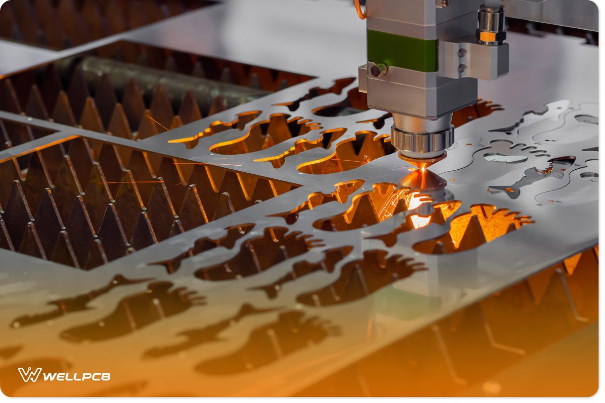
Methods of Creating an SMT Stencil
There are three main ways to create an SMT stencil:
- Laser cutting: A CNC machine directs a high-precision laser to cut the necessary shapes into a metal foil. Due to its accuracy and speed, laser cutting is ideal for high-density and fine-pitch components.
- Chemical etching: A photoresist is applied to a metal foil, exposed to UV light, and chemically etched, leaving the SMT stencil behind. While chemical etching is cost-effective and works well for larger aperture designs, it lacks the precision needed for small apertures.
- Electroforming: The manufacturer applies an aperture design to a mandrel, which is then used to build the stencil atom by atom through electrophoretic deposition. While complex, this method produces high-precision stencils with smooth walls and uniform thickness. Much like laser cutting, it’s ideal for fine-pitch components and productions that require high accuracy.
For cases that don’t require high-accuracy apertures for fine-pitch components, CNC-guided drills or punches may replace lasers..
Ultimately, your chosen method will depend on your budget, accuracy requirements, and scale of production.
2. Solder Application
Next, a solder paste printer applies solder onto the PCB pads through the stencil, marking where components will be placed.
After applying the paste, the manufacturer performs a solder paste inspection (SPI) using a machine equipped with cameras and sensors. The inspection ensures the applied solder paste has the correct shape, density, and alignment, which is crucial for creating strong solder joints in the final assembly.
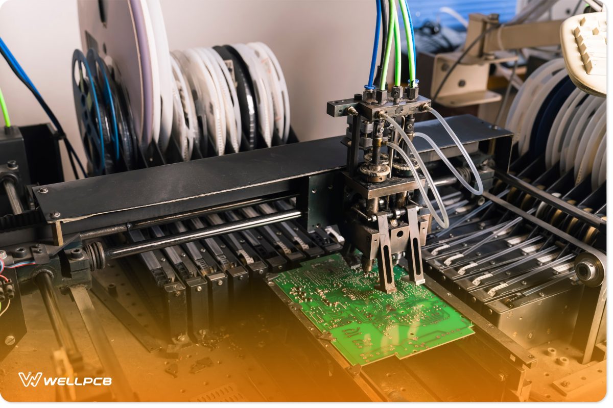
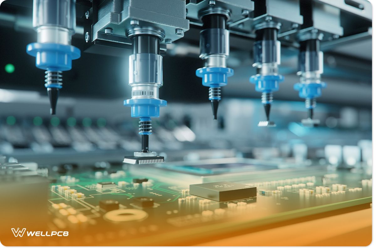
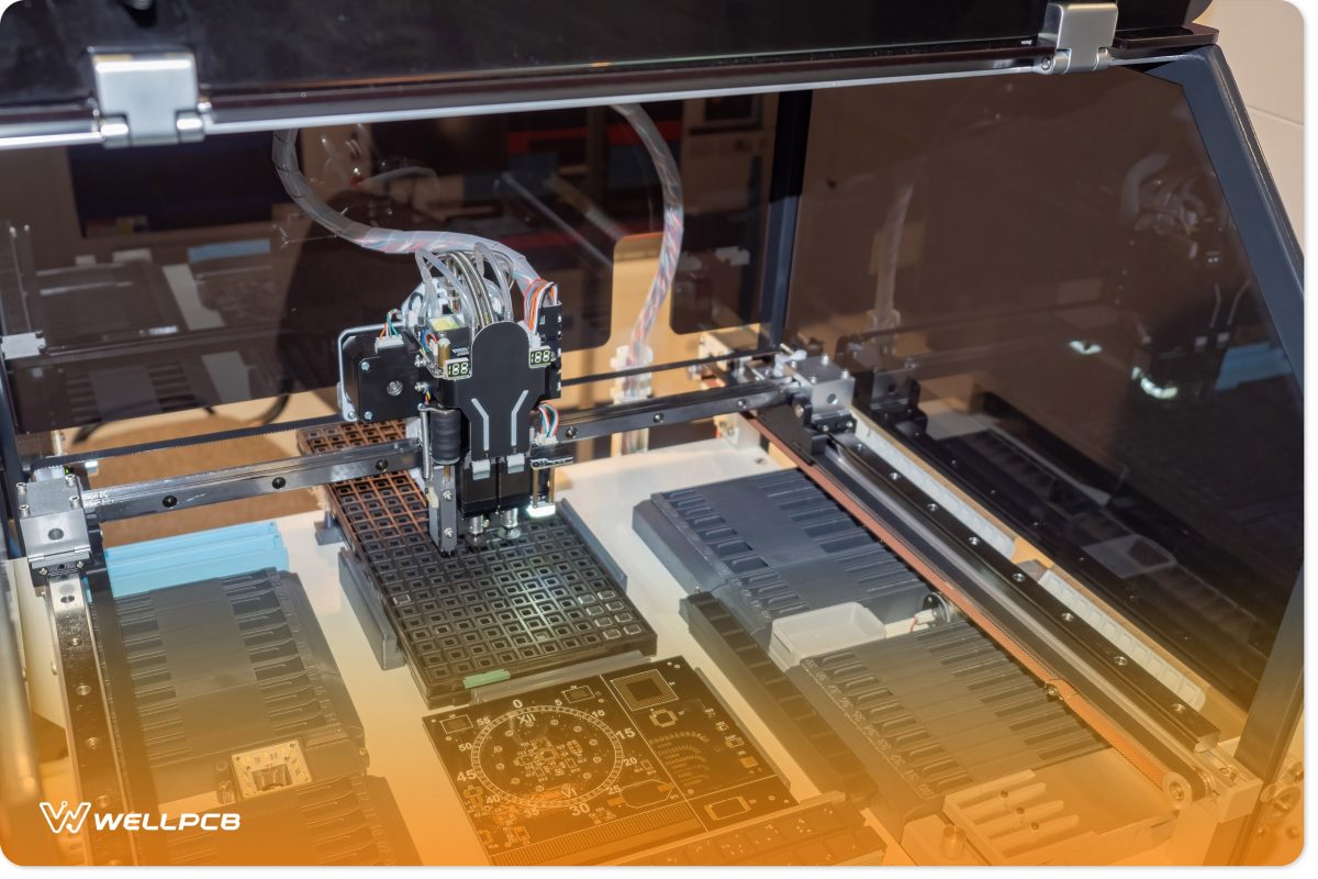
3. Component Placement
Pick-and-place machines then quickly and efficiently position the PCB components onto the solder-covered pads. While expensive, these machines are reliable and ultimately deliver perfect results.
Most pick-and-place machines use a conveyor system where feeders supply the components to a machine, which then uses nozzles to pick them up. Before placement, the machine aligns them carefully using a set of cameras and optical sensors. Once aligned, the machine places each component on the PCB, which is then moved along the conveyor belt for further processing.
For smaller productions, human operators may manually place components, though this is more time-consuming and carries a higher risk of error.
4. Soldering
Once placed correctly, the manufacturer solders the SMD components onto the PCB. The two main soldering techniques are:
- Reflow soldering: The PCB is heated in an oven to a temperature high enough to melt the solder paste, forming solder joints between the components and the PCB.
- Wave soldering: In this method, the PCB is passed over a pan of molten solder, which quickly forms solder joints. This technique is highly efficient and ideal for large production runs.
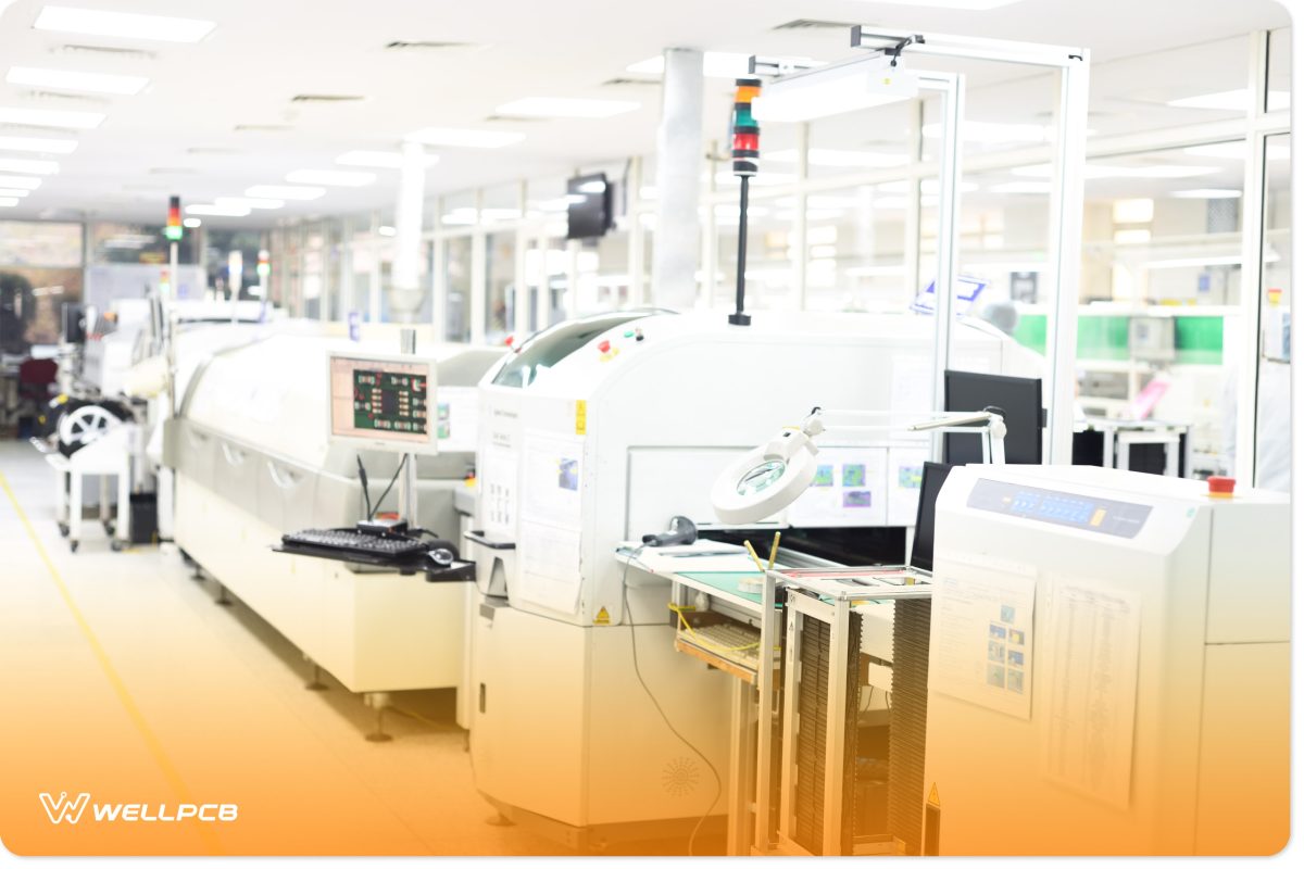
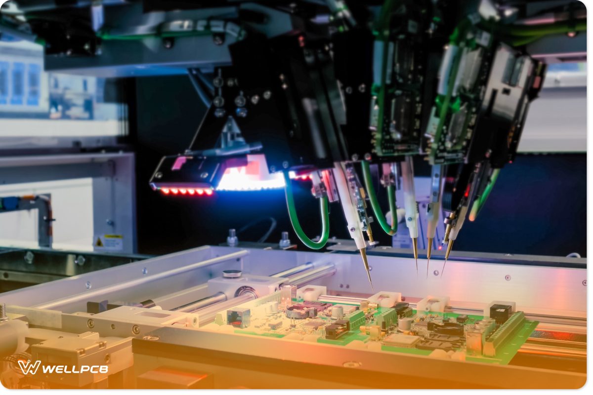
5. Inspection and Testing
Once soldering is complete, the manufacturer uses an Automated Optical Inspection (AOI) machine to ensure joint strength across the PCB.
AOI machines are equipped with sensors, cameras, and image-processing software to find any defects in the PCB assembly, such as misaligned or missing components. Once the machine confirms there are no defects, an operator moves the PCB to the cleaning stage.
During cleaning, residual flux and impurities are removed using a combination of water, solvents, and chemicals. This prevents corrosion and ensures the long-term reliability of the PCB assembly.
Finally, the PCB assembly undergoes functional testing using test fixtures and software. This ensures the PCB assembly meets all functional specifications and operates as intended. ures and software. This ensures that the PCB assembly meets all functional specifications and operates correctly.
What Are the Advantages and Disadvantages of SMT?
SMT offers a range of advantages that make it a popular choice in PCB assembly, but it also comes with certain drawbacks.
Advantages
1. Reduced Manufacturing Costs
SMT enables the design of smaller, more compact PCBs, which reduces material costs and manufacturing expenses. Due to their smaller footprints and lower profiles, SMT components can be placed closer together, maximizing the use of board space and minimizing waste.
2. Improved Work Efficiency
As most of the SMT process is automated, it minimizes errors and improves overall efficiency. SMT allows manufacturers to complete in a day what might take a week using manual methods. This increase in productivity shortens the time to market for electronics. This boost in productivity shortens the time-to-market for electronic products, reduces waste, and has the potential to increase profits.
3. Compact and Lightweight Designs
SMT-assembled boards are more compact and lightweight than those assembled using THT. SMT does not require extensive drilling, making the assembly process simpler and allowing for sleeker, more efficient designs.
Disadvantages
1. Mechanical Stress
Being smaller and more delicate, SMT components are more vulnerable to mechanical stress, which can weaken solder joints over time. These components are also more susceptible to damage during handling and assembly.
As such, manufacturers must perform thorough testing and inspection, but this can also be challenging due to the small component size. Issues like solder bridges, “tombstoning”, and weak solder joints are more common with SMT and require precision and care during assembly.
2. Environmental Concerns
The soldering process in SMT, especially methods like reflow or wave soldering, requires significant heat, which consumes large amounts of energy. This can be damaging to both the assembler and the environment.
3. Temperature Stress
SMT solder joints tend to be more prone to damage caused by thermal cycling—repeated exposure to varying temperatures during a PCB’s lifespan. Heating and cooling cycles can weaken the solder joints, potentially leading to failures over time.
4. Incompatibility with Certain Components
Designing for SMT PCB assemblies can be complex, as some components generate more heat and electrical noise than others. Due to the close proximity of SMT components, these effects can interfere with nearby components. This limits the range of components suitable for SMT designs and requires designers to pair thermally and electrically compatible components.
Future Trends in SMT
As technology advances, SMT is evolving to become more efficient and sustainable. Here are four SMT trends to keep an eye on in the near future:
AI and industrial IoT: AI and industrial IoT are transforming the SMT assembly process. AI-powered design tools help engineers create more efficient PCB layouts. Industrial IoT devices allow manufacturers to monitor and optimize assembly processes in real time. Supervisors can remotely survey multiple assembly processes, which improves productivity, efficiency, and accuracy.
Additive manufacturing (3D printing): Additive manufacturing is emerging as a valuable technology in PCB manufacturing. While today it’s primarily used for PCB prototyping, 3D printing has the potential to revolutionize SMT by enabling more sustainable and efficient stencil production.
Advanced reflow oven technology: A key disadvantage of SMT is its heat-intensive soldering process. Modern reflow ovens have improved temperature control, which not only conserves energy but also reduces the risk of damaging sensitive components. This allows for more efficient heating, addressing both environmental and quality concerns.
Lead-free solder alloys and fluxes: With the development of new solder alloys and fluxes, lead-free soldering has become more accessible and environmentally friendly. These materials often perform better and comply with regulations aimed at reducing harmful substances.
Conclusion
While SMT has seen significant technological advancements, it hasn’t fully replaced THT/PHT. This is because the industry has yet to overcome certain SMT limitations.
However, SMT continues to evolve, benefiting from innovations like advanced soldering materials, AI integration, and additive manufacturing.
These advancements make SMT more cost-effective, versatile, and less reliant on human supervision—which is particularly advantageous for large-scale projects.
If you’re considering SMT for your next project, staying informed on the latest trends and innovations can help you leverage its full potential.
To keep up with developments in the field, be sure to follow the WellPCB blog for regular updates and insights.


