Contents
What is a 4-layer PCB?
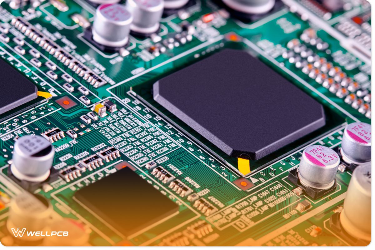
4-layer PCBs are printed circuit boards with four conductive layers.
These layers are sandwiched between two insulating layers, known as the substrate, and then laminated together to form a single board.
Compared to traditional two-layer PCBs, four-layer PCBs offer several advantages. The additional layers enhance signal integrity and improve thermal management, making them ideal for more complex circuitry.
Additionally, 4-layer PCBs are highly versatile and suitable for a broad range of applications. For even more adaptability, consider using a flexible PCB to meet specific design and space requirements in compact electronics.
4-layer PCB stackup
The stack for a standard 4-layer PCB is as follows: GND and VCC switch depending on the layer with the most signals.
Outer layers: These are the top and bottom layers. They are for routing signals.
Inner layers: These two inner layers are the two middle layers. They are to provide power and ground planes.
Then, we will talk about each layer in detail.
Layer one:
The bottom layer is typically made of copper. It serves as a foundation for the entire board and supports the other layers.
Layer two
This is the power plane, which provides a clean and consistent power source for all board components.
Layer three
It is the ground plane layers. It provides a clean and consistent ground source for all board components.
Layer four
This is the top layer. It is useful for routing signals and providing the connection points for components.
The function of the layers:
-signal layers
The signal layer is for routing signals. It is also where most of the components we placed are located. The inner signal layers are for routing high-speed or differential signals.
-ground and power plane layers
The ground and power planes provide clean and consistent power and ground sources for all components. Moreover, they help reduce noise on the board.
-solder mask layers
The solder mask is for protecting the copper traces from shorting and soldering. Besides, it provides a consistent and professional look to the board.
-wiring layers
The wiring layer is for connecting the different parts of the board. Plus, it provides structural support to the board.
-mechanical layer
The mechanical layer mounts the components to the board and provides support and stability.
-ground-layer/gnd layer
The ground layer provides a common ground for all the board’s components and helps reduce noise.
-reference layer
The reference layer provides a reference voltage for the board’s components and helps keep them stable.
-two additional routing layers
The 4-layer PCBs have additional routing layers. These layers are useful for routing signals between the different parts of the board and help reduce crosstalk.
Thus, 4-layer PCBs are very useful for a variety of applications.
-VCC layer
The VCC layer provides power to the board’s components and helps keep them stable.
Four-layer PCB benefits
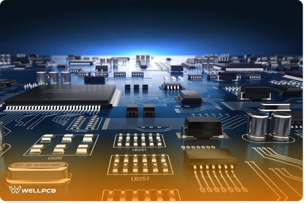
High-tech electronic PCB (Printed circuit board) with processor and microchips
A four-layer PCB provides many benefits over a traditional two-layer board. For example, the extra layers allow for better control of signal integrity and timing.
Moreover, they also provide increased routing options and improve thermal characteristics. Although 4 layer PCBs are more expensive than their two-layer counterparts, the benefits often outweigh the cost.
four layer pcb applications
Four layers PCBs are applicable in many areas, such as
- Automotive
Such as engine control, body electronics, and infotainment.
- Telecommunications
This includes the base station equipment, routers, switches, etc.
- -Consumer Electronics
Include 4K/HDR TVs, digital cameras and camcorders, Blu-ray players, etc
- Computer Peripherals
Such as printers, scanners, and mice
- Industrial Controls
This 4-layer PCB is used for programmable logic controllers (PLCs), lighting control, motor control, and security systems.
- Medical
This 4-layer PCB applies to diagnostic equipment, hearing aids, and patient monitors.
- And more!
If you are working on a project that requires high speed or precision, 4-layer PCBs may be the right choice.
2-layer vs. 4-layer PCB
During multiple layers, four layers and two-layer pcb are the most common. Regarding 4-layer PCBs vs. two-layer PCBs, knowing the difference is important to make the best decision for your project.
Here are some key points to consider:
– Cost
A four-layer PCB is more expensive than a two-layer. The increase in layers increases the overall price of the board.
This is because more material is necessary, and manufacturing is more complex.
– Designs
A four-layer PCB can be useful for more complex designs than two layers because there is more space to work with, and more features can be included.
PCB vias are also more important in 4-layer PCBs. They can connect different layers and make the design more flexible.
-Functionality
Four-layer PCBs usually have more functionality than two-layer. This is because they can support more complex designs and include more features.
One example is that 4-layer PCBs can support higher-speed signals, as the extra layers can be applied to route the signals faster.
A 4-layer circuit board can also support more power and ground planes because the extra layers can be useful for routing the power and ground planes.
In addition, 4-layer PCBs can also support more trace widths and spaces. This is because the extra layers can route the trace widths and spaces.
Besides that, 4-layer PCBs can also support more copper thicknesses. That is because the extra layers can be applicable to route the copper thicknesses.
-Comparing the Processes of Prototyping
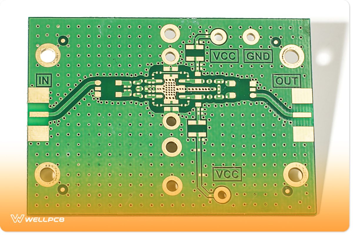
Prototype printed circuit design
For prototypes, 4-layer PCBs are the best way to test your design before going into production. They can also support more trace widths and spaces.
You can use the extra layers to route the trace widths and spaces.
Also, 4-layer PCBs can support more copper thicknesses. This is because the extra layers can route the copper thicknesses.
-Stack ups Compared
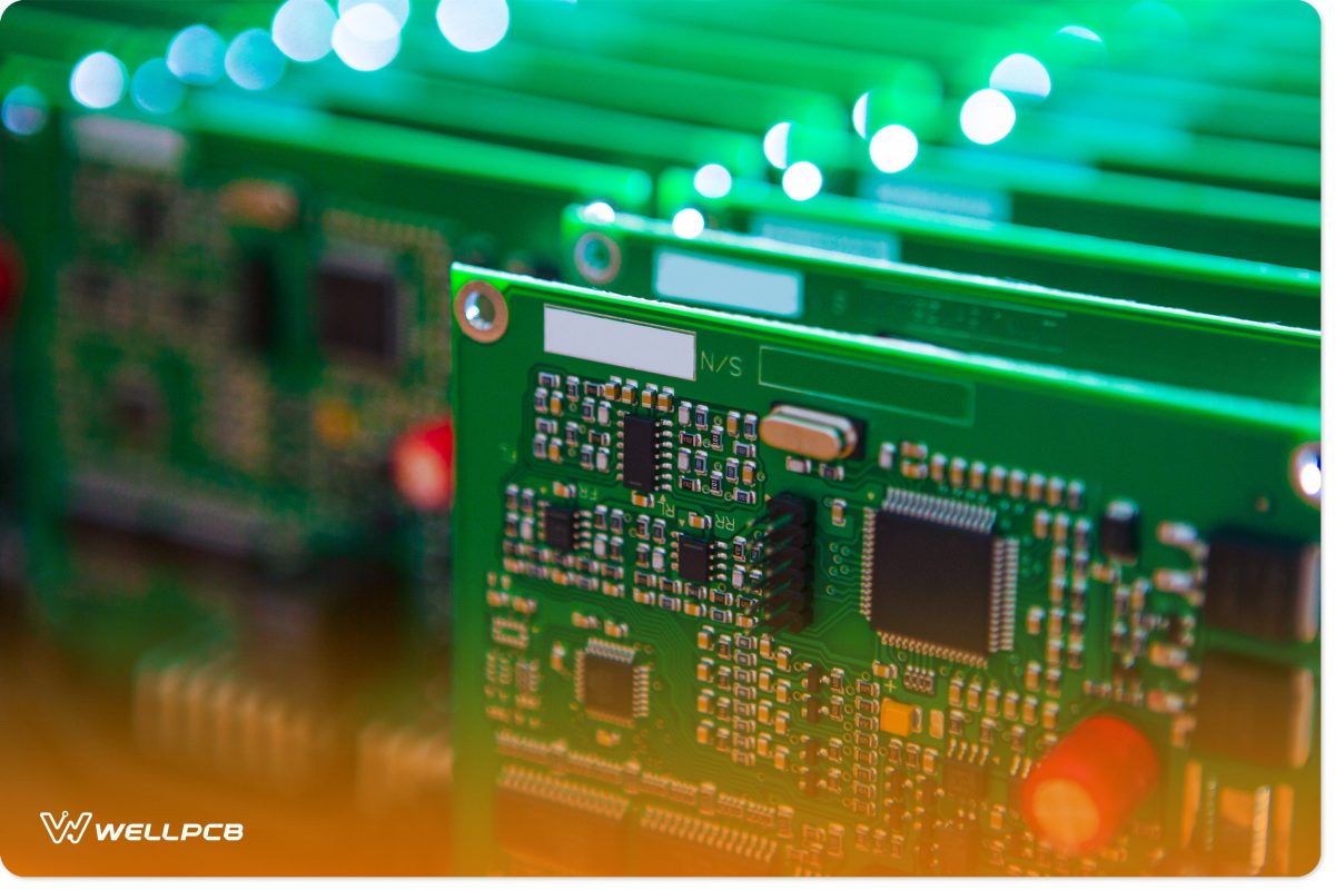
green embedded microcircuits
Compared to the two-layer circuit board, four-layer PCBs offer many benefits that the former can’t provide. In addition, four-layer PCBs allow for smaller trace widths and spaces.
They also support a wider range of copper thicknesses and more silkscreen colors. Four-layer PCBs also have better mechanical strength.
4-layer PCB price
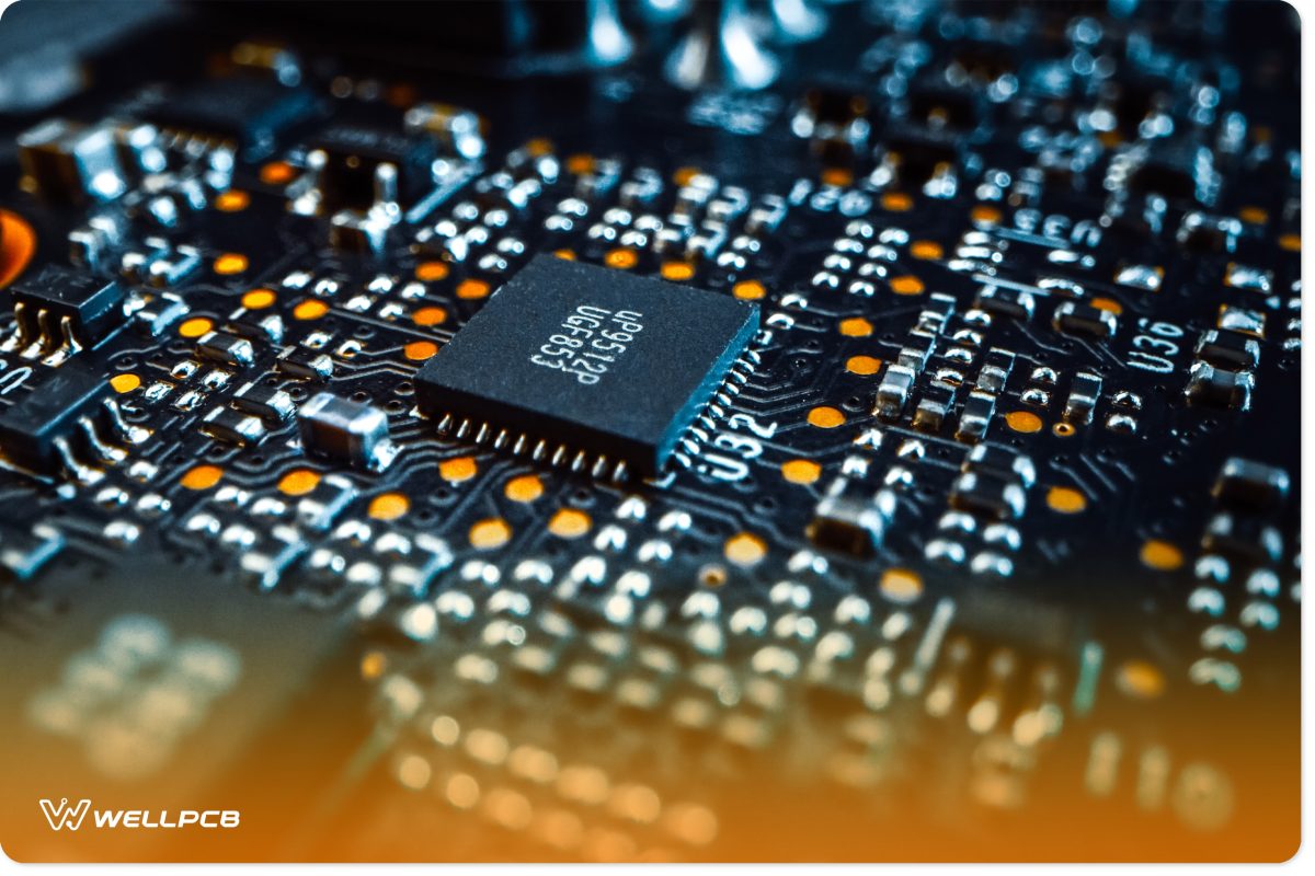
Macro Close-up Shot of Circuit Board with Computer Motherboard Components
4-layer PCB price depends on many factors, and the following:
-Board size
Firstly, you should consider the board size. As the size of 4 4-layer PCBs varies, the larger 4-layer PCBs will cost more.
– Layer count
Then, the four-layer board needs more materials. As a result, it will cost more than the double-sided boards.
– Material used
Thirdly, 4-layer PCBs use multiple materials, and the cost of each material is different. Therefore, the price of a 4-layer PCB varies from $38 to $100.
– 4 layer pcb complexity
Moreover, four-layer PCBs are more complex than double-sided boards, so they require more time to design and manufacture.
Thus, the price of four-layer PCBs is also higher than that of double-sided boards.
– Copper thickness
Also, you should note that 4-layer PCBs generally have thicker copper than double-sided boards, which contributes to their higher price.
– Surface finish
In addition, a 4-layer PCB generally has a better surface finish than a double-sided board. This is because a 4-layer PCB can have more layers of copper, which can provide better support for the surface finish.
4-layer flex PCB
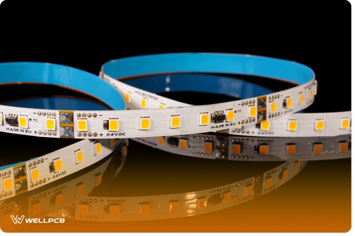
LED flexible printed circuit board strip for various lighting applications
4-layer flex PCB is a kind of 4-layer PCB made of flexible material. However, a 4-layer flexible PCB is more expensive than a four-layer board but has many advantages.
Pros of the four-layer printed circuit board.
Orange flex circuit board with white connector and reflection on a black background.
- Firstly, a 4-layer flex PCB is more flexible, and it can be bent or folded, which is very convenient for various applications.
- Besides, the 4-layer flex PCB is also more vibration-resistant and shock-resistant, making it ideal for harsh environments.
- In addition, 4-layer flex pcb is more heat-resistant and can withstand higher temperatures than 2-layer pcb.
Although 4-layer flex pcb is the best choice for many applications, it is more expensive than 2-layer pcb.
4-layer PCB Thickness

Computer board with visual effects in a futuristic style
How thick is a 4-layer PCB? You may wonder about this.
The thickness of a 4-layer PCB is generally 0.13-0.15mm, but a thicker 4-layer PCB is also available with a thickness of 0.20-0.25mm.
Moreover, 4-layer flex pcb can be made even thinner with a minimum thickness of 0.05mm.
4-layer PCB Manufacturing Process
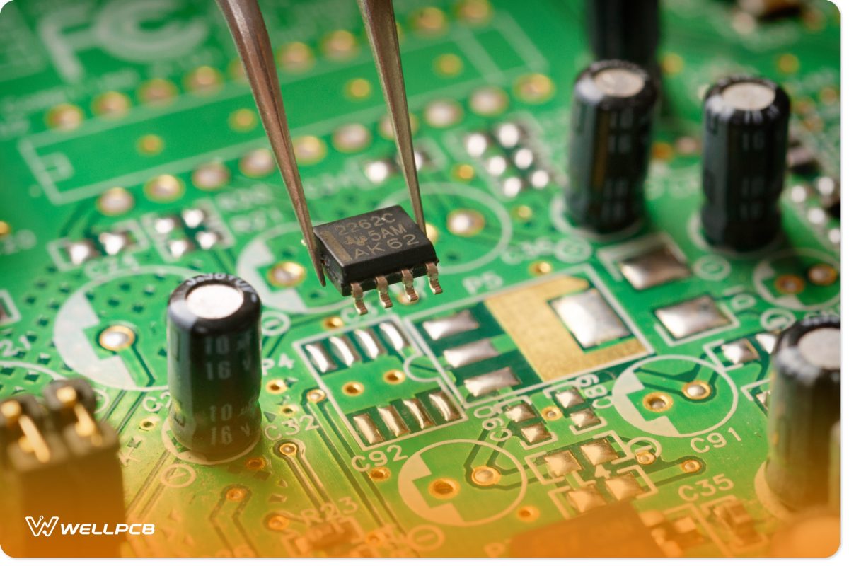
Assembling a circuit board
The 4-layer PCB manufacturing process is as follows:
– The first step is to create the inner layers.
This involves laminating the inner layer stackup, drilling, and milling vias. And then adding any plated features such as pads.
– The second step is to create the outer layers.
This involves laminating the outer layer stackup together and drilling and milling vias.
– The third step is to assemble the 4 layers.
This involves bonding the inner and outer layers using a special adhesive.

Close-up view of man looking at circuit board through a magnifying glass
– The fourth and final step is to finish the 4-layer pcb.
This involves adding final plated features, such as solder masks or silkscreens. Once the 4-layer PCB is complete, it is ready for use in your electronic device.
As you can see, 4-layer PCBs are more complex than your typical two-layer PCBs. But with the help of a professional 4-layer PCB manufacturer, you can get the 4-layer PCBs you need for your next project.
4-layer PCB manufacturers
Fantasy digital room with electronic components in the interior
There are many 4-layer PCB manufacturers to choose from. But how do you know which one is right for your project?
Here are a few things to consider when choosing a 4-layer PCB manufacturer:
– Price: You want to find a 4-layer PCB manufacturer that offers a competitive price. So be sure to get quotes from several manufacturers before making your final decision.
– Quality: Quality is important when it comes to 4-layer PCB manufacturing. Therefore, finding a 4 layer PCBs manufacturer with a good reputation for manufacturing high-quality PCBs.
Delivery: When it comes to 4-layer PCB manufacturing, you’ll want to find a manufacturer that can deliver your PCBs on time. So be sure to ask about lead times when getting quotes from 4-layer board manufacturers.
– Minimum order quantity: Many 4-layer circuit manufacturers have an MOQ, so be sure to find the MOQ for the 4-layer PCB manufacturer.
– Service: Last, you’ll want to find a 4-layer PCB manufacturer that provides good customer service.
With these things in mind, you should be able to find a 4-layer PCB manufacturer that is right for your project.
Summary
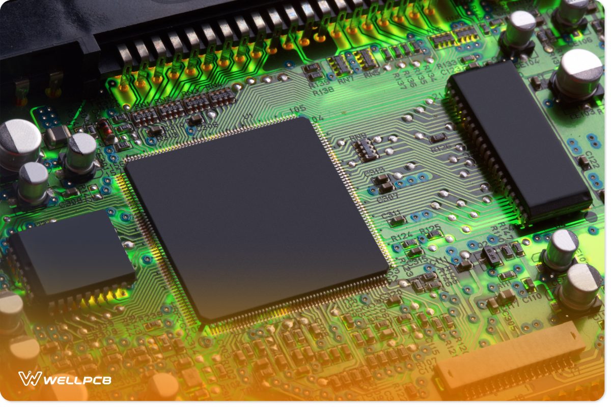
Circuit boards populated with some components
PCB fabrication is a complex process that can be difficult to understand. We’ve walked you through the basics of each layer and what happens during the fabrication process.
Now that you have a basic understanding, it should be easier to communicate with your fabricator about your project.
If you still have questions or need help getting started, our team is here to assist you.
We look forward to working with you on your next PCB project!


