Contents
Gold Fingers PCBs
1.1 Definition
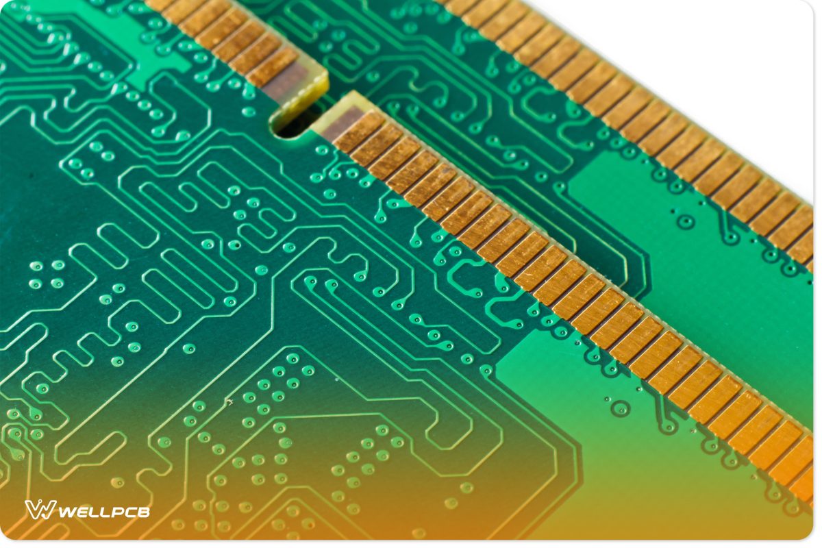
As outlined before, “Gold-finger PCB” refers to gold-plated connectors mounted at the interconnecting edges of a periphery PCB.
Other names for a Gold Finger PCB are a Gold Connector, Edge Connector, Edge-Board Connector, Connector Finger, Contact Fingers, Gold Taps, or Gold Tips.
You, too, might have interacted with Gold Fingers PCBs in the past.
Wait, can you remember interacting with a collection of shiny-looking, finger-like projections on the edges of a joining end of a peripheral circuit board?
Aha! That’s what I am talking about here. They resemble fingers in the sense that they look thin and elongated at the contact edges of a PCB.
Gold Fingers are usually fitted onto the edges of periphery PCBs or prototype boards to enhance connectivity with larger boards.
The edge connectors (i.e., gold fingers) are also plaited with flash gold (hard gold) with a thickness that varies between 3u’ and 50u’ (units in Micro Inches).
1.2 Why Gold Plaiting Is Necessary For Gold Fingers PCB
PCB connection points are subject to constant plugging and unplugging owing to their nature of interconnecting PCBs.
Hence, without a strong contact edge, they are prone to wear and tear that can cause device malfunction.
Plaiting the connectors with other metals (in this case, gold) enhances the durability of the edge connectors.
But I am sure you might have wondered: of all metals, why should edge connectors be gold-plated? Isn’t gold too expensive?
Couldn’t copper conduct better and be a lot cheaper than Gold?
Well, I have an answer: sure, gold plating of gold fingers is expensive, but it is necessary.
Gold was chosen over other metals because, so far, it has proven to have high corrosion resistance, high electrical conductivity (second to copper and silver), and the ability to be alloyed with cobalt or Nickel to increase its resistance to wear and tear.
Earlier experiments that were done to establish the resistance of gold vis-à-vis its resistivity and compared to other popular metals showed that.
Gold had a lower resistance than other metals, as shown in Table 1 below.
| Contact Material | Resistivity (Ωcm) | Contact Resistance (mΩ) |
| Pure Gold | 2.4 X 10⁻⁸ | 0.8 |
| An alloy of Gold and Cobalt | 2.4 X 10⁻⁸ | 2.6 – 2.8 |
| Palladium on Nickel | 1.08 X 10⁻⁷ | 3.1 – 5.8 |
| Silver | 1.6 X 10⁻⁸ | Non-determined |
Gold is also inert. It does not oxidize or react readily with other metals.
This property of gold makes it an ideal choice for making parts that are prone to exposure or likely to react with other metals.
Even though silver is sometimes useful, it is not recommended for commercial production as silver is susceptible to sulfide and chloride attacks.
In the current market, there are two main types of gold plating for gold fingers. These are:
- Electroless Nickel Immersion Gold (ENIG): ENIG is cheaper to acquire and more comfortable to solder than hard gold. However, it is softer and cannot withstand constant plugging and unplugging without wearing out. It is recommendable for experiments and prototypes, but it is not a good option for commercial usage.
- Hard-plated Gold over Nickel: Hard-plated gold over Nickel is harder and thicker than ENIG. It is most suitable for commercial applications.
In recent applications, most manufacturers have used a combination of the two types of gold plating techniques to strike a balance between the efficiency of the electronics and a lower cost of production.
1.3 Chapter Overview
So far, we have learned that gold finger PCBs are gold-woven edge connectors of periphery PCBs to other PCBs.
We have also covered some main reasons why gold plaiting is necessary for the connector fingers.
In the remaining part of our edition, we will learn how to make gold finger PCBs, their applications, and the standards that guide their production.
In our next chapter, we will learn to make gold finger PCBs.
How Are The Gold Fingers Sorted?
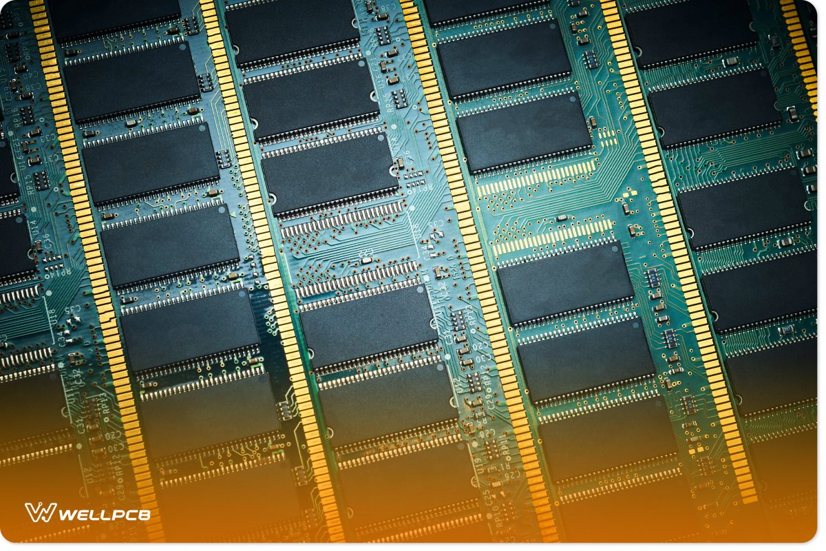
Image of RAM with gold fingers.
Gold fingers come in three different types, and each connects the same way.
Regular

Gold fingers on a GPU.
This type has solder pads (even length/width) at the PCB’s edge. Graphic cards are an example that use regular gold fingers.
Long-short
A long-short one contains different-sized gold fingers. It works with card readers, memory modules, and USB drives.
Segmented
The segmented gold finger is slightly different because it has a detached front section.
Differences Between PCB Gold Fingers And Gold Finger Connector
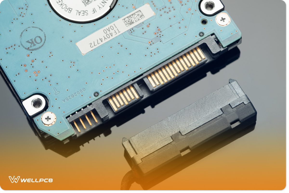
A hard drive adapter.
Both of these aren’t the same—and you can tell how exactly by looking into them. The table discusses each.
| Gold fingers | Gold finger connector |
| It goes on the edge of the device, component, or circuit board. | You will find these on any part of the circuit board. |
| They use hard gold for plating, which means you’ll pay more when the PCB is made. | This stays on the PCB, which means the duty cycle is lower. |
| They use hard gold for plating, which means you’ll pay more when the PCB is made. | A plastic housing protects it, so the gold finger connector is much cheaper to manufacture. |
| They use hard gold for plating, which means you’ll pay more when the PCB is made. | They use hard gold for plating, which means you’ll pay more when the PCB is made. |
| With the hard gold plating, it comes with better conductivity and is harder to damage over time. | The thermoplastic box stores each socket. You can find all the pins along the border of the circuit board. |
How Do You Make Gold Finger PCBs?
The essential step in manufacturing gold fingers is gold plating or layering other metals on PCBs.
This requires the raw PCB to be plated, a plating bar (image below), and plating specifications.
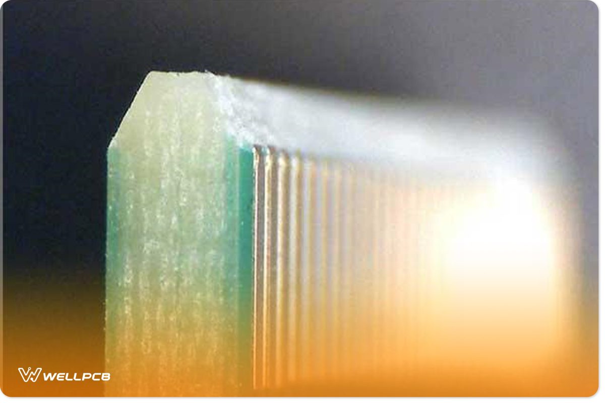
We apply gold after the solder mask process during PCB manufacturing and gold plating.
Most of the time, we perform surface finishing for the rest of the board before gold-plating edge contacts.
The process described below assumes that you have already acquired a PCB and only seek to gold-plate its edges to enhance its durability. It involves the following steps:
2.1.1 Steps Involved In Ordinary Gold Plating:
- First plate between three and six microns of Nickel to the edge connector fingers
- Add between one and two microns of solid gold (preferably gold alloyed with some cobalt) layers to the fingers.
- Bevel the layers carefully to ease the insertion of the board into its slot. Most modern designs of PCBs specify beveling level/height. If it is not specified, you can ignore it.
2.2 Making Other Types of Gold Finger PCBs
Because of improvements in Gerber and PCB designing, edge connectors have evolved to have different designs to suit different manufacturing goals.
Two popular PCB gold fingers are the unequally sized edge connectors and the segmented gold fingers.
2.2.1 Unequally Sized Gold Finger PCBs
In some cases, some fingers are intended to be shorter than other fingers within the same PCB.
An excellent example of such a PCB is the one used to manufacture traditional memory card-readers (as shown in the image below).
The logic in making some fingers shorter than others is that the components linked with the long fingers must be powered before those connected to the shorter fingers.
2.2.2 Making Segmented Gold Fingers
Segmented gold fingers are used to connect PCBs of most modern hybrid electronics.
They are composed of fingers that vary in length and some that are segmented, i.e., disjointed within the same fingers of the same PCB.
They are common on water-resistant and rugged electronics.
Steps To Making A Segmented Gold Finger PCB
The production of non-water gold and gold finger plating process is very similar to the standard gold finger production already discussed.
However, in this case, one is required to increase precision cleaning the segments.
A summary of the steps is:
Preparation of ENIG/ hard gold → Character Formation on plating bar → Gold Finger Plating → Laser Drilling (the process of segmentation) → Dusting/Cleaning → Sharpening → Electrical testing
Take Note!
1. To ensure that the gold fingers align exactly with their respective edge connector profiles on the joining boards, you will need to route the vertical edges of the connectors on their first plating run.
2. When doing this process manually, you will need to keep edging out any spillage or excess when adding layers of the finishing material to maintain the fingers’ shape.
2.3 Limitations of Gold Finger PCB Technology
Even though gold finger technology is of great importance, its application is still limited in that:
- Plated pads must be on the edge of a PCB. Because gold plating involves an electroplating process, a connection must link the plated pads with the connection panel frame.
- Most plating pads are limited to producing gold fingers that do not stretch over 40mm. In case you might need to have longer gold fingers, the process of manufacturing them might increase.
- The inner layers of the edge connectors have to be free of copper. Otherwise, the process of beveling the contacts might expose the copper.
4. Except for flexible PCBs, the minimum separating distance between the upper and lower layers of a PCB when plating on both sides is supposed to be 150mm.
In the remaining chapters, we will examine the uses of Gold Fingers in the industry and their limitations.
Applications & Limitations of Gold Finger PCBs
The uses of PCB gold fingers can be divided into both technical (applications on circuits) and industrial/commercial applications. Let us begin with the Technical application of the contact fingers
3.1 Technical Applications Of Gold Finger PCBs
Within the circuit, PCB gold fingers have several uses. Some of the technical applications of the connectors are:
1. They connect a PCB to a power source: one of the primary uses of the contact fingers is to connect a module PCB to a power source on the connecting profile of a larger PCB.
2. They help transfer signals/data: primarily, gold fingers link with the other PCBs to ease the transfer of data and signals between the peripheral PCB and the larger board.
3. They interconnect modules within the same board: traditional electronics used to consist of several robust modules that could not be interconnected easily within the same board. With the aid of flexible PCBs, electrical engineers could interconnect multiple modules even within the same board.
4. They provide room for future improvements: well, imagine a computer motherboard without ports and expansion slots.
What would it look like? How would it function?
And would other interested electricians improve it without adding expansion slots or vendor modules? The picture is unimaginable.
You would not be able to connect input devices and output devices.
Other engineers would not have worked on the improvement of a computer’s keyboard or mouse or VGA card.
Simply put: without having gold finger PCBs, machines cannot be improved.
3.2 Commercial applications
In the industry, gold fingers PCBs are used in several areas. Some of the popular applications include:
1. They provide connections for data transfer on network-enabled devices. I.e., we apply Gold fingers to manufacture network cards and other additional networking PCB modules.
2. They are used to attach specialty adapters. Edge connectors provide an attachment area for special adapters like Video Graphic Array (VGA) cards and other video cards that are useful in processing images.
These additional specialized modules relieve the main board of some useful processing when computing.
3. They connect other devices to the main processing board. In addition to the advantage of connecting network modules and specialized adapters, you can also use gold finger PCBs on the connecting edges of peripheral devices that get connected to the main boards.
Their application is relevant in the production of devices like Memory card adapters/readers and flash drives, among others.
These additional devices can help boost processing, add storage memory, or power the main board.
4. They are also used to connect audio adapters to main PCBs.
Regulations, Guidelines & Standards
Currently, the most popular standards that guide the production of PCB gold fingers are those released by The Institute for Interconnecting and Packaging Electronic Circuits.
The organization later transformed into The Association for Connecting Electronics Industries (IPC).
In 2002, IPC released its earliest standards of gold fingers.
The IPC-4552 standards 2002 focused on guiding the plaiting process of printed circuit boards and PCB finishing.
Later, in 2012, they were amended and improved 2012 to the IPC-4556 standards.
Then again, of all their releases, the IPC A-600 and IPC-6010 standards of 2015 are still the most popular standards for gold finger manufacturing in the current market.
Here is a summary of some of the guidelines for manufacturing gold fingers:
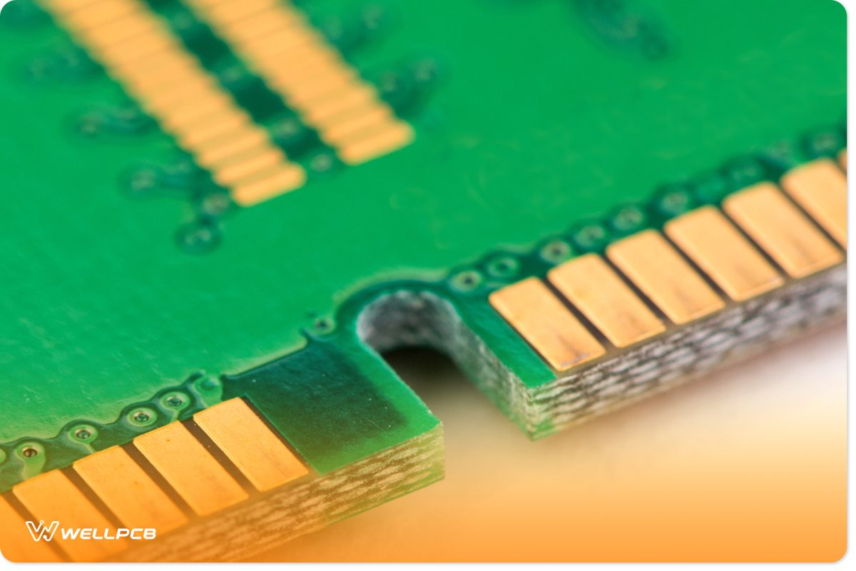
1. Visual inspection of contact edges:
The edges should be clean and have a smooth texture under simple investigation with the aid of a magnifying lens. They should not possess extraneous plating or “Nickel’s foot.
2. Finishing thickness and size:
The layers of the gold fingers should be measured to ensure that the thickness ranges between 3u’ and 50u’ (units in Micro Inches).
The standard thickness sizes currently are 0.031′, 0.062′, 0.093′, and 0.125′. For prototypes, we use the lower bound of thickness, and for boards intended for use in areas that require constant plugging and unplugging or excessive force of insertion, we use the upper bound.
The copper weight for the inner finishing layer is 1 oz. while that of an exterior finishing was proposed as 2 oz.
3. Tape testing of contact edges.
The tape test is the most straightforward test for determining the adhesiveness of gold fingers.
The standards recommend a “tape test” to establish the adhesiveness of the plated material on the gold fingers.
In carrying out the test, a strip of tape is applied to the contact fingers and removed.
Upon removal, the tape is carefully examined to see if traces of the plating materials remain.
Any show of the plated material on the tape indicates poorly plated contact fingers.
4. Chemical composition:
The gold used in electroplating should contain at least 5%—10% cobalt. This combination helps to boost the rigidity of the contact edges.
Even though we have summarized some of the simplest tests you can carry out to conform to IPC standards, several other guidelines outlined by the standards still guide our production of commercial gold fingers.
As professional PCB manufacturers, we are committed to conforming to the latest standards that ensure the safety and efficiency of the electronics we offer our clients.
FAQs
What is meant by gold finger connection?
This just refers to the interface that connects devices with the PCB. This ensures that data, power, and signals can move between the two.
Which electronics contain gold fingers?
There are so many devices out there with gold fingers. You’ll see that video cards, RAM, a computer’s motherboard, etc, all have it.
Do gold fingers need special materials?
Gold fingers consist of gold, but a cobalt or nickel alloy may cover them to make them stronger and last longer.
Conclusion
A small manufacturer finds it challenging to produce standard PCBs that meet IPC standards for safety and efficiency.
Precision is paramount, and timeliness is also critical in such projects. Perhaps you have been wondering how you will navigate the production puzzle.
Don’t worry; if you wish to have your PCBs manufactured in full conformity to IPC standards at a tremendous bargain and delivered in time, feel free to make an online PCB quote with us.
As professional manufacturers, we are dedicated to helping you produce better electronics by having superb PCBs.
Also, consider checking out our website for more information and offers on PCBs.


