Contents
Custom PCB Printing Design
When designing custom-printed circuit boards, the first step is to create a schematic. A schematic serves as a blueprint, outlining how the components will connect and work together effectively.
To create a schematic file, you’ll need to use a software tool suited for the task. Selecting the right tool is crucial for accurately capturing your design intentions and ensuring a smooth transition to circuit board manufacturing.
A lot of custom-printed circuit board manufacturers prefer using :
2 KiCad
3 Quadcept
Based on the fact that it is highly optimized when it comes to optimizing custom printed circuit boards. For example, with Quadcept, you can quickly export the Bill of Materials directly, and since it is cloud-based, you can conveniently use this software almost anywhere.
Of importance to note is that there are also other software tools to choose from, such as:
1 ExpressPCB
2 Upverter
3 PADs
4 ORCAD
5 DipTrace
6 Cadence Allegro
Out of the many custom printed circuit board design software that designers may use, some are highly used based on their full functionality.

Custom PCB Printing Layout
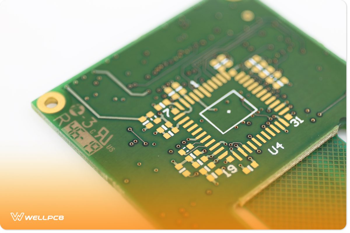
The next thing to be aware of when it comes to custom-printed circuit boards is your board’s layout. To design the perfect arrangement, you can rely on the same software tools mentioned above. However, unlike schematics, your custom printed circuit board’s layout is all about allocating the parts to the actual location on the printed circuit board. It is also crucial to show the traces that connect every component between the printed circuit board layers.
As you may be aware, the higher the number of layers you choose to have on your custom-printed circuit board, the more complex and challenging to style it will get. The layout of a printed circuit board demands the technical expertise of experienced professionals who have been in the field for a long.
A reliable printed circuit board layout also demands the knowledge of essential things such as :
the aided design system, custom printed circuit board design software, or other skillful methods required to transfer necessary components needed towards the design of the final printed circuit board. When thinking about the layout of your printed circuit board, you need to factor in essential aspects such as :
1 The layers you need
2 The size of your board
3 Pair routing, sketching
4 Drawing a custom printed circuit board outline
5 3D modeling, to mention but a few.
Gerber Files For Custom PCB Printing
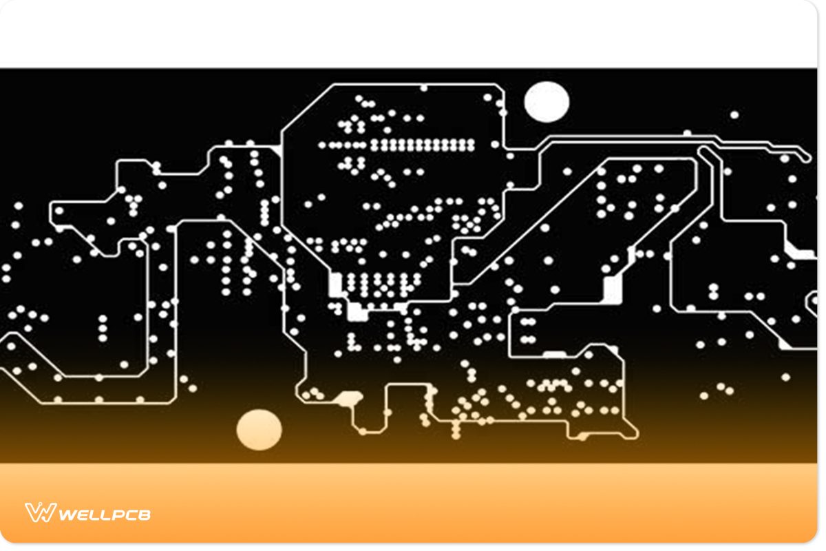
When it comes to manufacturing printed circuit boards, you may hear designers mentioning Gerber files from time to time. Gerber files are computer-aided design files sent to the producers of printed circuit boards to develop the layer structure of the printed circuit board. In short, a Gerber file is an image of the printed circuit board that showcases every individual layer as they will appear throughout the circuit design. They represent images of copper layers, legend, solder mask, and route data that simplify viewing how the circuit board requires fabrication.
Gerber files come into play after completing the layout design of printed circuit boards, and printed circuit board manufacturers use such data. There are plenty of printed circuit board manufacturing firms out there that offer these services, WellPCB being one of them.
The moment you get to send your Gerber files to a printed circuit board manufacturer of your choice, they will be able to print out the circuit board. Printing out your circuit board becomes the basis for manufacturing up even further. With Gerber files, you can effectively add components to your custom PCB printing board with a lot of ease.
Custom PCB Printing Material
Material Type:
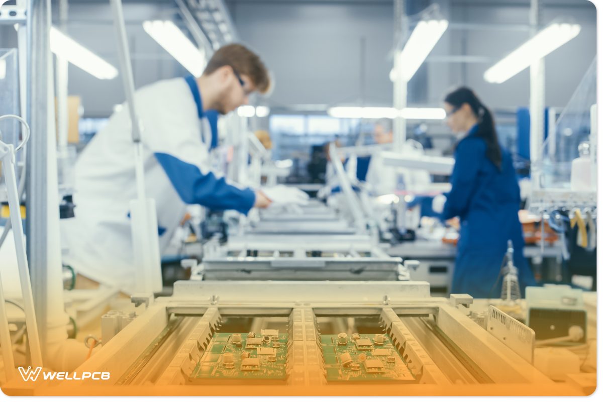
Regardless of the mindset behind manufacturing any device, you need to consider the type of materials you’ll use. When it comes to the manufacture of custom PCB printing, there are several components used here. Some of them are Led-emitting diodes (LEDs) that allow current to flow through them, but only in one direction. Other vital components in printed circuit boards are resistors.
Optimize component materials:
Resistors function by controlling or regulating the current to minimize their value. There’s also the battery, transistors, switches, diodes, and inductors. All these are essential component materials that go into the design of a printed circuit board. When preparing documents, you can either go ahead or inquire from your PCBA manufacturer to make the order for you if you find it hard doing so, or do it on your own if you already have the vendors selected.
Component number and order quantity:
Some of the things that you need to keep at the back of your mind when selecting components include component type number, optimized parts, packaging, lead time, and the minimum order quantity, among other things. For example, if you think of purchasing less than the required components, you need to check your minimum order quantity by making sure that your selected parts are entirely in stock. Additionally, in terms of lead time, you need to keep in mind that some ingredients may take from 8-16 weeks to reach you.

Cost-effectiveness Of Custom PCB Printing
A printed circuit board design engineer must consider all the aspects that may impact the total cost of manufacturing a printed circuit board, especially custom PCB printing. More often than not, custom-printed circuit board designers who are new on the job fail to consider the costs associated with manufacturing them.
Some of the things that can impact the cost of manufacturing custom printed circuit boards that a majority of designers fail to plan for include things such as tooling costs, the spacing of board parts, and the size of the printed circuit board. But to ensure the cost-effectiveness of your custom-printed circuit board, you need to look at the costs of tooling, the materials that you’ll use on your custom-printed circuit board, and the number of layers, among others.
To ensure that you significantly minimize your manufacturing costs, you may have to manufacture small-size printed circuit boards. Also, you may have to select simple shapes of a PCB instead of going for complicated forms. Still, you can choose to use readily available materials instead of expensive materials, some of which may require some importing.
Custom PCB Printing Board Thickness
There are plenty of factors that come into play when manufacturing and custom PCB printing. Some of them include their weights, profiles, and parts of the board. However, some of the most important factors to consider consist of the thickness of the printed circuit board. But why, you may ask.
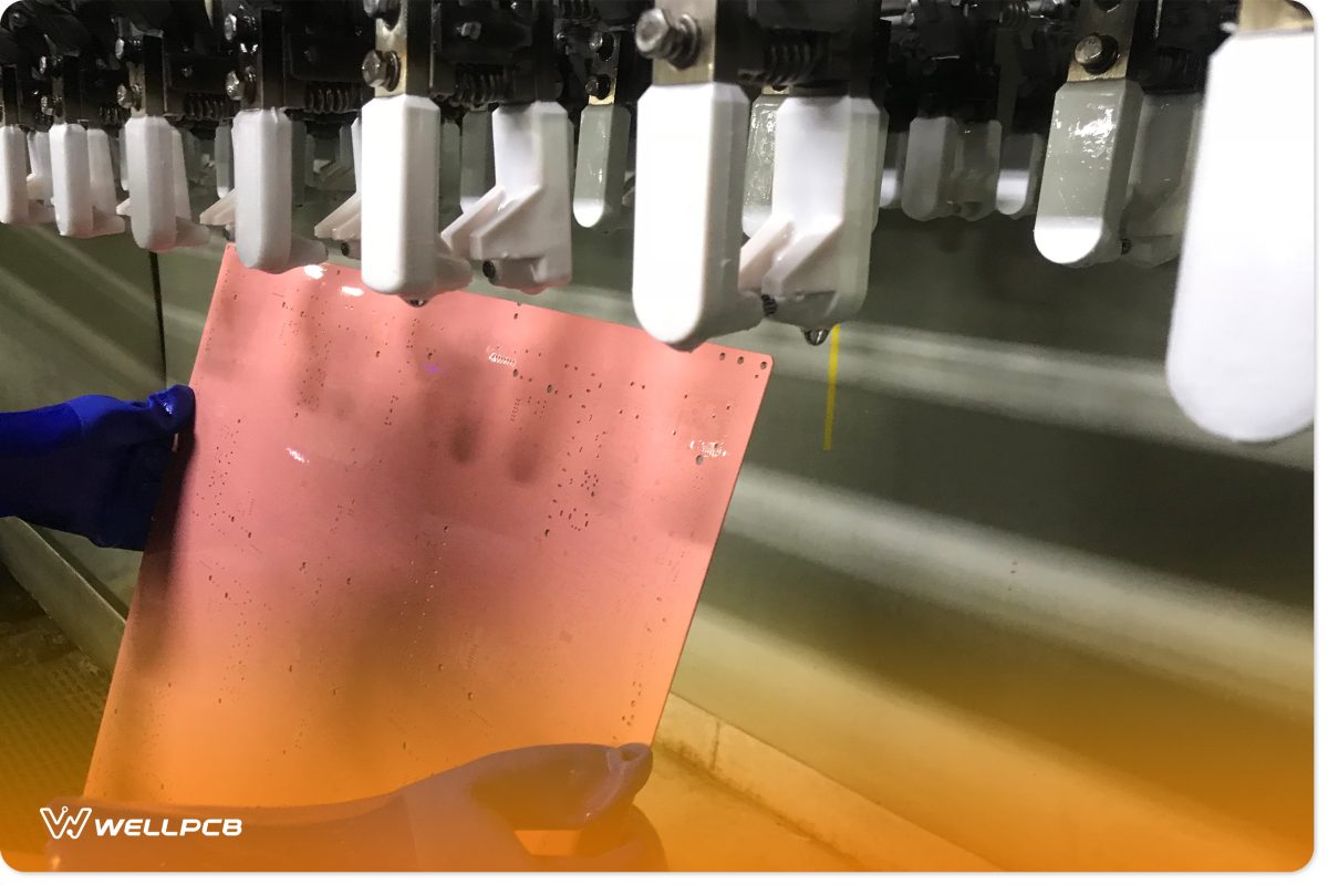
The printed circuit board’s width does affect its resistance and conductivity, which are some of the primary considerations that need to match the requirements of your printed circuit board. The thickness of your printed circuit board plays a vital role in its functionality. Several levels of depth are available, such as the standard thickness, standard Fr-4 thickness, standard core thickness, and standard two-layer thickness.
Summary
We at WellPCB have experience in custom PCB printing. As we promised at the beginning of the article, our mandate is to ensure that you don’t just get the right vendor but find the best from what they have to offer you.
You don’t want to hesitate on this matter any longer, as we at WellPCB are right behind you. Just give us a call, and we will go ahead and do the rest. At your earliest convenience, contact us and see how you can go about securing products made of the latest technology.


