
Contents [hide]
What Are Flexible PCBs?
Flexible PCBs are circuit boards that easily flex, twist or bend without breaking. Flexible printed circuits (FPCs) have printed circuit patterns on a thin polymer film substrate. This flexible substrate allows the flex PCB to adapt to many different shapes for the desired application.
All the circuit traces and components are coated by a thin polymer, ensuring protection against harsh environments. For high-quality production, professional PCB manufacturing services provide tailored solutions to meet the unique demands of flexible PCB applications.
The main three differences between flexible and rigid PCBs are:
- Flexible PCBs are foldable and bendable due to their material composition, typically polyester or polyimide. Rigid PCBs have a flat base and can’t bend or flex. They are made from stiff materials like fiberglass (FR-4), which makes them more durable.
- Flexible PCBs are less durable than rigid PCBs but they can withstand movement and vibrations better than the rigid type.
- Flexible PCBs are generally thinner and lighter than rigid PCBs.
Types of flexible PCBs
- Single-sided flex PCBs consist of a conductive layer set on a dielectric polyimide film. Components and circuits are placed on one side of the PCB.
- Double-sided flexible PCBs have two conductive layers. The components and circuit are integrated on both sides.
- Multi-layer flex PCBs have at least three conductive layers. Due to the complex manufacturing process, they are also the most expensive type.
How Are Flexible PCBs Used Everyday?
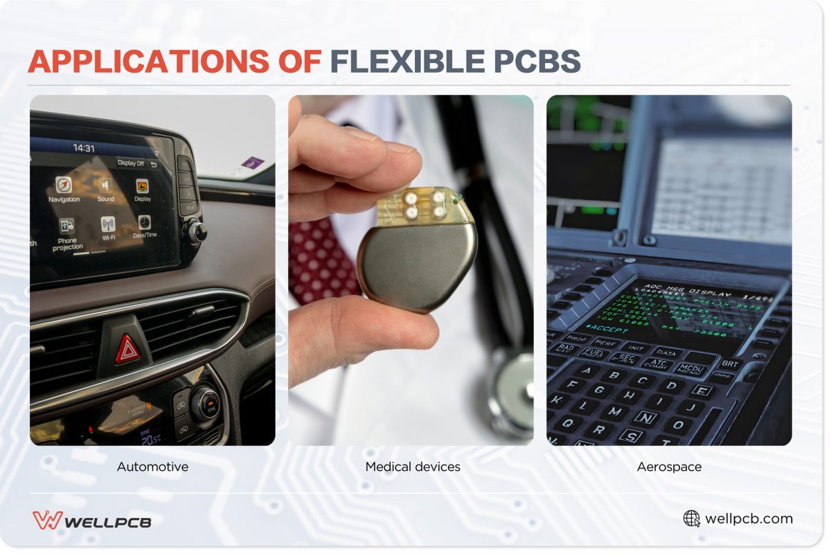
Applications of Flexible PCBs
Because of their versatility, convenient size and ability to handle robust electronic conditions, they have a wide range of applications in many different industries. Their robust design makes them ideal for high-density applications.
Automotive
The automotive industry uses flex PCBs in many circumstances. Some popular applications include:
- airbag deployment units
- engine control units and sensors
- infotainment systems (such as in Tesla’s Model S vehicle)
Flex PCBs are beneficial as they can handle a vehicle’s high temperatures, shock, and continuous vibrations.
Medical devices
Flex PCBs are useful in medical devices due to their size and flexibility. They are used in applications such as:
- hearing aids and cochlear implants
- pacemakers
- endoscopic tools
For example, medical technology company Medtronic uses flexible PCBs in its tiny transcatheter pacing device. It provides reliable, long-term pacing therapy for arrhythmia patients.
Medical devices using flex PCBs are more biocompatible, which means they are more likely to work inside the human body. Plus, the flex PCB has a smaller profile for smaller medical devices such as implants. They also ensure wearable devices are more comfortable for patients.
Aerospace
Aerospace uses flex PCBs for avionics and flight systems as they’re more reliable for environments with fluctuations in temperature, vibration, and air pressure. This industry generally uses them for:
- jet engine control modules
- flight display
- navigation systems
Boeing’s aircraft feature flex PCBs in navigation and control systems, which operate in extreme weather conditions.
Flexible PCBs fit within aerospace equipment’s compact spaces due to their small size, adaptability, and capacity for movement. They’re also incredibly lightweight, leading to component weight reduction and performance boosts.
What Are the Steps Involved in the Flexible PCB Manufacturing Process?
The process for manufacturing flex PCBs is different from the rigid PCB manufacturing process.
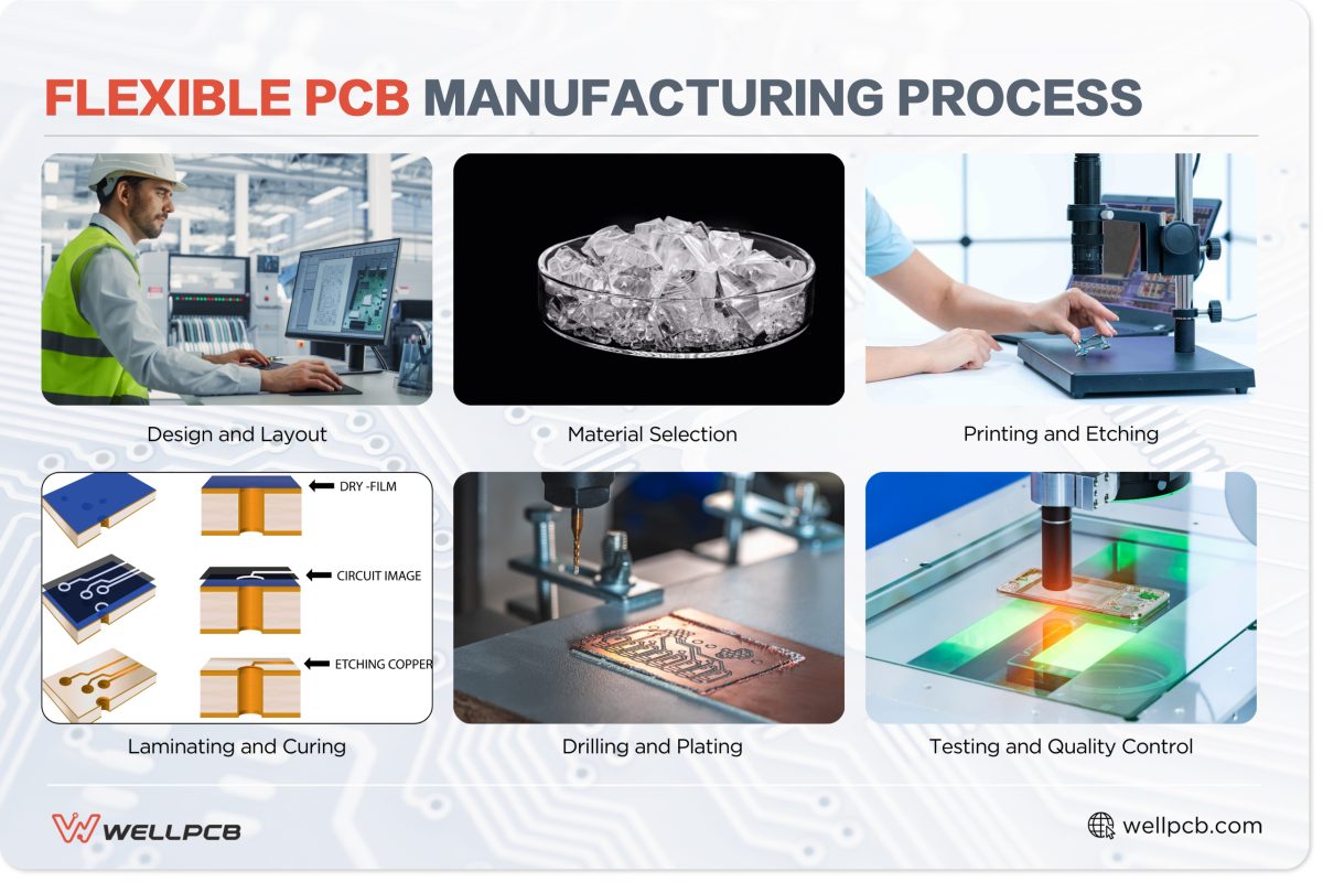
Flex PCB manufacturing process
Step 1: Design and Layout
The design phase ensures the flexibility, durability, performance, and reliability of the flexible PCB. If the design parameters are met, the PCB should flex without performance or integrity loss.
CAD and EDA software tools are used for flex PCB design and development. Some of the most common ones used are:
Computer-aided design (CAD) tools
- KiCAD: KiCAD is open-source and loaded with features like a 3D viewer, component library, schematic capture, and PCB layout.
- Altium Designer: This user-friendly software has advanced features like simulations and 3D visuals for easier flex PCB design processes. It features error-checking capabilities.
- Eagle: Eagle makes it easy for users, including beginners, to design schematics and circuitry. The PCB design software is bundled with SPICE simulation for output testing.
Electronic design automation (EDA) tools
- Cadence Allegro features signal routing, HDI structures, and microwave topologies. It also incorporates AI to achieve quick layout and routing designs.
- Mentor Graphics PADS features signal integrity analysis tools, analog and mixed-signal design simulations, and routing automation.
- Zuken CR-8000 enables multi-board system designs. It also features 3D visualization tools for flex PCB design and analysis. This EDA software supports HDI designs, too, for compact circuits.
What Should You Consider in Your Flexible PCB Design?
- Materials: Polyimide and polyester are the most popular material choices for flex PCBs. Select one based on the circuit’s application requirements and choose adhesive-less material.
- Bend radius: Consider the bend radius to keep the substrate and conductive paths undamaged due to mechanical stress. Select the recommended bend radius based on layer counts to ensure the PCB doesn’t break.
- Trace routing: Rounded conductive traces avoid stress hotspots that occur from sharp angles. This ensures stress doesn’t accumulate in one region, which may cause mechanical damage or failure. Efficient trace routing eliminates short circuit and electrostatic discharge risks.
- Layer stack-up: Take the number of stacked layers into account. The fewer layers the PCB has, the more flexible it becomes.
- Components and vias: Consider where the PCB components will connect. Integrating them away from bend zones reduces circuit stress. Add vias in stress-free regions to prevent damage.
Step 2: Material Selection
Polyester (PET) and polyimide (PI) materials are used in flexible PCB manufacturing. These exhibit flexibility, thermal resistance, and electrical insulation.
| Polyester | Polyimide | |
| Temperatures | Ideal for low to moderate temperatures (-40°C to 150°C) | Handles temperatures reaching 250°C or higher. Consider a material with high thermal stability, like polyimide. |
| Performance | Polyester is best for standard circuits since it has a lower dielectric constant and thermal stability. | High-frequency circuits need polyimide as it has low dielectric loss and low permittivity. |
| Durability | For applications with minimal mechanical stress. | Better for applications requiring improved durability as it can withstand continuous strain or stress |
| Flexibility | Better for applications with low to moderate bending or flexing. | Wearables and similar use cases. |
| Chemical resistance | Low chemical exposure. | High chemical and moisture resistance qualities for outdoor or industrial use. |
Step 3: Printing and Etching
Manufacturers use two techniques to print and etch the circuit onto the substrate.
Photolithography
- First, the substrate is cleaned to eliminate contaminants like dust or dirt. Then, the material substrate is covered with a light-sensitive photoresist, which solidifies after light exposure.
- The photomask with the circuit design is positioned above the substrate. Circuit patterns are on the clear and obscure parts of the photomask.
- Afterward, the photomask and substrate are exposed to ultraviolet light. It passes through the photomasks’s clear regions and turns the photoresist solid.
- Soft photoresist parts are taken off, and the hardened parts remain. A chemical solution soaks the uncovered regions, etching the circuit pattern onto the flexible substrate. Remnants of the solid photoresist are finally removed.
Digital imaging
- The substrate is cleaned before being covered with a photoresist. Afterward, a computer-controlled laser scans the photoresist to expose the circuit pattern onto the substrate.
- This develops the exposed photoresist. Now, the circuit pattern is on the substrate, which undergoes etching to form the circuit features.
- The leftover photoresist is removed after etching, showing the circuit pattern on the substrate.
- Precisely transferring the circuit pattern onto the substrate enables correct component placement. Extreme precision leads to accurate conductive trace formations, boosting PCB performance. Otherwise, abnormalities create problems like short and open circuits.
Step 4: Laminating and Curing
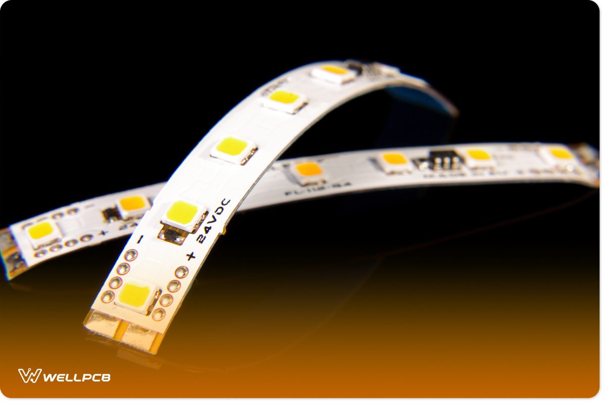
flexible printed circuit board strip
The lamination and curing process sets the circuit on the substrate.
Lamination
- First, the copper foil and flexible layers are cleaned. An adhesive layer is then applied between each flexible layer before aligning and stacking them together.
- In a vacuum-like setting, a lamination press exposes the stacked layers to heat and pressure. Changing the temperature and pressure helps the adhesion set while keeping the substrate damage-free.
- Lastly, the stack cools, hardening the adhesion that securely bonds each layer.
Curing
Curing helps with performance stability and device durability for long-term use. There are several curing techniques.
- Ultraviolet (UV) light: Specially formulated adhesives cure quickly with UV light, which hardens the material upon exposure.
- Thermal: In this curing process, an oven or IR (infrared) evenly heats the laminated flexible layers, hardening the adhesive.
- Microwave: Microwave radiation is suitable for thick layers as the energy infiltrates the material to make the adhesive solid.
Quality control is vital during this step. Internal defects can be detected by using X-ray or ultrasonic imaging. Meanwhile, peel tests determine the adhesion bond’s strength. Visually inspecting the stack is a good way to find defects, including delamination, bubbles, or misalignment.
Step 5: Drilling and Plating
Drilling and plating form the electrical connections of the circuit.
Drilling process
- Manufacturers place the flex PCB between two support materials like phenolic or aluminum sheets for stability.
- Computer numerical control (CNC) machines and lasers drill small holes in the flexible material. Micro drill bits make small vias holes.
- Stacking multiple panels can help with drilling efficiency. An additional board goes underneath the stack, protecting the bottom panel from damage.
- Afterward, the drill bit fragments are cleaned with a special vacuum system, keeping the holes clear.
Drill types
Manufacturers rely on mechanical drills for large holes. A carbide mechanical drill is suitable for tougher substrates because it maintains sharpness and durability throughout usage.
CO2, YAG, and Excimer lasers precisely drill holes in flexible materials. CO2 produces bigger holes, YAG makes small, fine holes, and Excimer drills tiny, precise holes.
Plating techniques
- Through-hole plating: Electrical interconnections between each layer are created by evenly chemically plating the drilled holes with copper.
- Electroplating: The flex PCB is submerged in an electrolyte with copper ions. A current is applied, forcing those copper ions on the hole walls and uncovered copper surfaces.
- Vertical continuous plating: This technique ensures uniform copper thickness on walls of plated through-holes. It’s achieved by vertically soaking the PCB in chemical baths.
- Pads-only plating: A process where a photoresist protects the PCB while the vias and padding get plated.
Step 6: Testing and Quality Control
Testing the flexible PCB ensures it doesn’t have defects. It verifies the performance, safety, and reliability of the circuit board. Flex PCB post-production tests include electrical testing, thermal testing, and flex testing.
Electrical testing
Electrical testing involves using automated test equipment (ATE) to measure the impedance, capacitance, continuity, and resistance. This method is precise and efficient for performance and functionality testing.
Additional parameters are also checked, including waveform, stability, signal delay, and amplitude.
Thermal testing
Manufacturers use thermal testing techniques to determine if the flex PCB can withstand harsh temperatures.
Heat dissipation testing evaluates whether components can disperse heat in operational use. The technique also determines if the components could overheat.
Thermal cycling tests ensure the flex PCB withstands sudden temperature fluctuations. They expose the circuit to repetitive heating and cooling cycles.
Flex testing
Bend testers determine if the PCB handles flexing or twisting. Sometimes, this test is repeated to evaluate the PCB’s durability and reliability after continuous use.
Dynamic flex testing involves constantly bending the flexible PCB to see if it stays undamaged. Bend radius testing demonstrates the PCB’s ability to bend to a certain radius without damage or failure. Static flex testing subjects the PCB to frequent angular bends, holding it there for a long time.
Quality control standards and measures
Quality control is performed by visually inspecting the board for defects like misalignments. Meanwhile, automated optical inspection (AOI) relies on cameras and software to find defects.
Manufacturers use these standards to determine if the PCB has high performance and efficiency:
- ISO 9001: Manufacturers refer to this quality management standard as a guideline for their products. It helps to affirm the flex PCB satisfies customer and regulatory specifications.
- IPC-6013: This standard is representative of the flex PCB’s performance requirements.
How are Flex PCBs Beneficial?
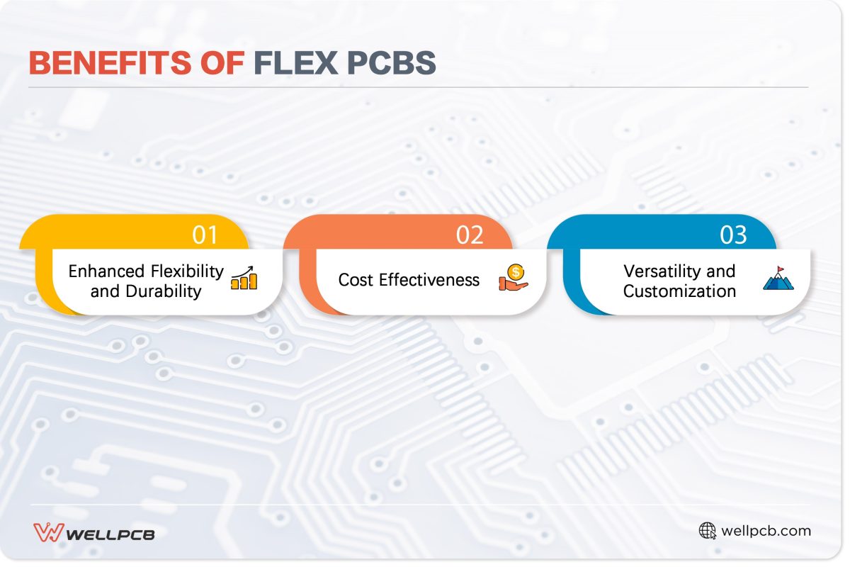
Flexible PCBs have advantages that have revolutionized electronics, including:
Enhanced Flexibility and Durability
Flexible PCBs bend due to their material composition, unlike rigid PCBs. Their small size makes them ideal for lightweight devices exposed to lots of movement, changes in temperature, and other variables.
For example, the flex circuit is ideal for fitness trackers as they require frequent movement and agility.
Their biocompatibility also makes flex circuits more practical for long-term use in medical implants.
Cost Effectiveness
Flexible PCBs’ small size eliminates unnecessary component and connector integration, slashing production costs.
They don’t need much maintenance due to their robustness, resulting in long-term savings.
However, the manufacturing costs can be higher than rigid PCBs due to the materials and processes.
Versatility and Customization
Flex PCBs are versatile as they conform to tight spaces by twisting to a desired shape.
These are customized based on requirements like layer counts, materials, and components.
A reliable 300-foot flexible PCB was designed for precise temperature measurements.
Another example involves a vehicle heater with a few components, leading to a 40% cost reduction.
What Are the Industry Innovations and Trends in Flexible PCB Manufacturing?
Thanks to high-density interconnect and fine-line printing technology, components are integrated into more compact spaces, allowing miniaturization.
Laser direct imaging (LDI) and roll-to-roll (RTR) lamination improved flex PCB production, enhancing precision.
Other materials like advanced composites, graphene, and conductive polymers enable better flexible PCB performance.
These advancements reduce costs and boost innovation in industries like IoT, aerospace, and the automotive industry.
Biocompatible flex PCB demand could skyrocket. As stretchable electronics become more popular, this may lead to a boom in flexible PCB productivity for applications in flexible displays and soft robotics.
Eco-friendly materials and practices could soon be adopted due to stricter regulations.
This can prioritize customized, flexible PCBs, rapid prototyping, and low-volume production.
Get Started with Our Flexible PCB Manufacturing Services
WellPCB is committed to providing high-quality and innovative flex PCB manufacturing solutions.
We use the best practices and required standards to meet customer satisfaction on every project.
Are you ready to choose expert flex PCB fabrication for your next project? Contact us today to work with our experts.


