
Contents
- 1 How Does PCB Manufacturing Technology Work?
- 2 What are the Latest Advancements in PCB Manufacturing Technology?
- 3 What Are the Benefits of Adopting Advanced PCB Manufacturing Technologies?
- 4 What Industry Trends and Future Directions Can We Expect to See in PCB Manufacturing?
- 5 What Is Our Commitment to Innovation and Quality?
How Does PCB Manufacturing Technology Work?
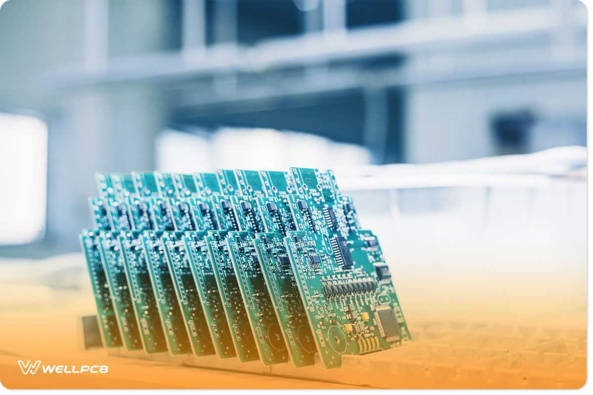
Computer boards
PCB manufacturing technology encompasses the hardware, software, and methods used in the design, fabrication, and assembly of printed circuit boards.
It all started in 1956 when the US Army published the first patent for the circuit assembly process. Back then, this was primarily a manual process carried out by human operators.
As PCB technology became more widespread, its production became increasingly demanding and complex. As a result, manufacturers developed proprietary techniques to optimize fabrication and assembly, reducing errors and improving quality.
This is why many of today’s PCB production processes are automated and computer-guided. For modern, efficient solutions, professional PCB manufacturing services leverage advanced technology to meet today’s quality and precision standards.
What Are the Key Technologies in Modern PCB Manufacturing?
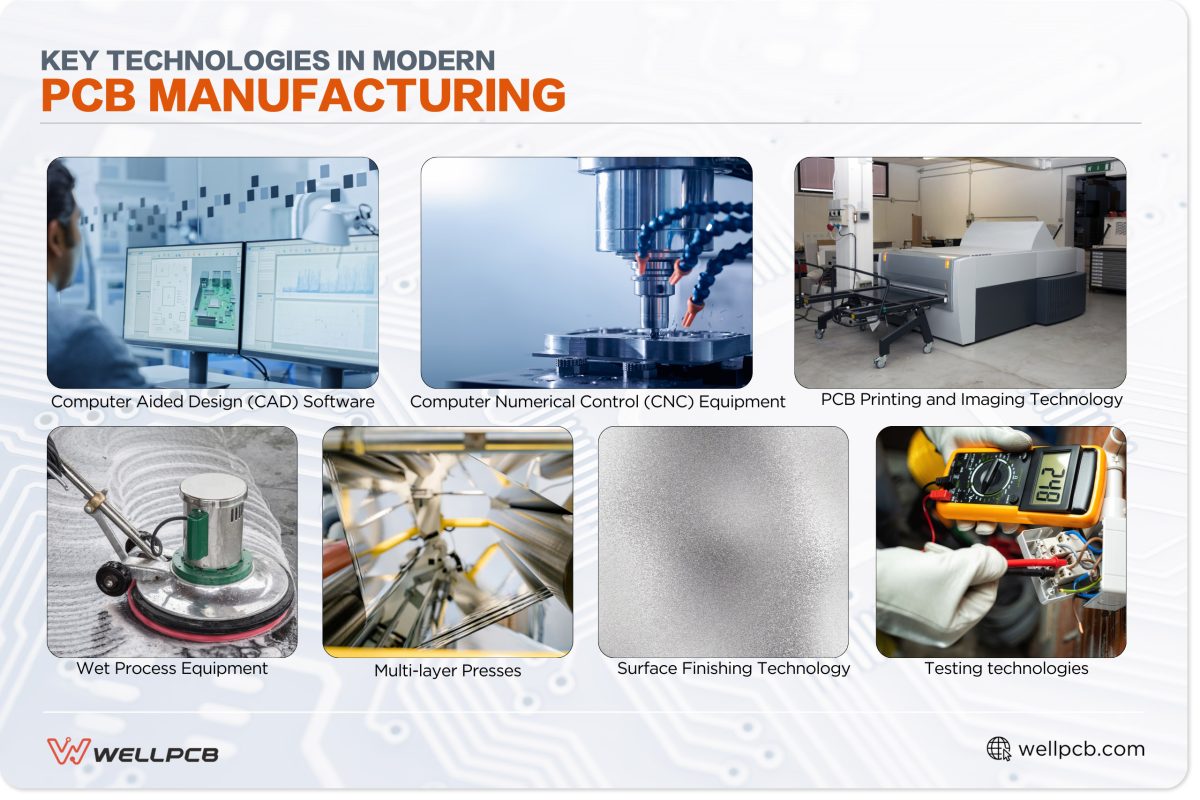
Key Technologies in Modern PCB Manufacturing
PCB manufacturing is a complex, multi-stage process, and each stage relys on specialized tools and technology. Here are the key technologies that define modern PCB manufacturing.
- Computer Aided Design (CAD) Software: This software enables the design and generation of PCB outlines and blueprints. Today’s CAD software often incorporates machine learning and AI, helping designers adhere to production guidelines and minimize errors.
- Computer Numerical Control (CNC) Equipment: CNC equipment consists of highly precise, computer-controlled tools used in etching and drilling processes. This category includes scoring machines, routers, lathes, drills, and mills, all of which are operated automatically by computers.
- PCB Printing and Imaging Technology: This technology covers plotters, film processors, lamination, curtain coating equipment, and legend and screen printers. Many of these machines require minimal human supervision, as they are largely computer-managed.
- Wet Process Equipment: These machines handle cleaning and solderability preparation. Examples include brushing machines, plasma treatment machines, direct plating machines, chemical cleaning machines, resist developers, solder mask developers, and galvanic lines.
- Multi-layer Presses: These are laminating hydraulic machines used for multi-layer PCB fabrication. Modern multi-layer presses are computer-managed, providing more precise control over values like temperature and pressure.
- Surface Finishing Technology: This category includes machinery used to prepare and apply surface finishes to PCBs. Examples include HAL, immersion silver, ENIG, and galvanic nickel application lines.
- Testing technologies: This refers to various testers and tools used to ensure the functionality and quality of PCBs. This includes automated optical inspection systems, electric testers, X-ray analyzers, and copper thickness measuring systems.
Many PCB manufacturers also use neutralization machinery and techniques to safely manage and dispose of the waste produced by the various chemical processes involved in PCB manufacturing. These technologies are essential to minimize the environmental impact and ensure compliance with relevant regulations.
What are the Latest Advancements in PCB Manufacturing Technology?
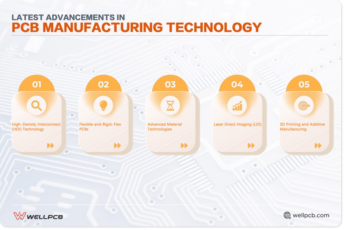
Latest Advancements in PCB Manufacturing Technology
High-Density Interconnect (HDI) Technology
High-Density Interconnect (HDI) PCBs are advanced multi-layer boards with a higher density of connection pads than standard PCBs.
Despite their trace density, HDI PCBs have similar surface area and dimensions to regular PCBs. This is due to innovative and savvy design decisions.
For instance, consider that HDI PCBs feature fine tightly packed trace lines. Because this layout creates space constraints that don’t permit the insertion of regular-sized vias, manufacturers have had to use miniaturized vias, known as microvias.
Along with capture pads, microvias allow manufacturers to selectively connect and route the various conductive layers of the HDI PCBs.
This means that HDI PCBs can fit more components on a single board without jeopardizing functionality or longevity.
While HDI PCBs are more expensive to manufacture, they’re more powerful and are suitable for compact design form factors. As such, you’ll find them in various small high-performance devices, such as laptops, Mini-ITX motherboards, smartphones, and gaming consoles.
Graphics cards, or GPUs, are a notable example of the modern impact of HDI technology.
Companies like Nvidia, which projected record revenue of just under $70 billion in 2024, heavily rely on HDI PCBs to support the complex integrated circuit (IC) of its GPUs.
These GPUs are critical for data centers, where they facilitate machine learning and AI technology.
This underscores how advancements in PCB manufacturing technology drive innovation across the tech industry.
Flexible and Rigid-Flex PCBs
Flexible and rigid-flex PCBs are another example of PCB technology that’s made compact, high-performance devices possible.
These PCBs are lightweight and can bend and conform to tight spaces, making them ideal for applications where size and weight are critical factors.
These characteristics make flex and rigid-flex PCBs indispensable in the production of medical devices, wearables like heart rate monitors, and specialized aviation and military hardware.
Advanced Material Technologies
Innovation in PCB manufacturing isn’t limited to structure and design, as there have been significant advancements in material technology.
Manufacturers increasingly use robust materials with improved insulation and better signal capacities.
For instance, HDI PCBs often use advanced materials like BT Epoxy Resin or Polyimide with non-woven aramid reinforcement, which can easily be drilled with lasers to form microvias.
Environmental and performance considerations have also led to changes in material selection.
The industry has largely moved away from toxic materials like lead-based surface finishes, opting instead for gold-based finishes like ENEPIG and ENIG. These are more environmentally friendly and produce better overall results.
Additionally, substrate materials like Polytetrafluoroethylene (PTFE) are now preferred for high-frequency applications due to their low dielectric loss, making them ideal for use in radar systems, wireless communication devices, and high-precision sensor and alarm systems.
Laser Direct Imaging (LDI)
The imaging process outlines the circuit traces on a PCB. Unlike traditional photo exposure, laser direct imaging (LDI) uses a concentrated light beam to carve out these traces.
LDI is fully computer-controlled, making it more precise and efficient than older photolithographic processes. It also tends to be more cost-effective, requiring fewer materials and less supervision.
LDI-produced images also tend to have higher resolution, enhancing the quality of the PCB.
3D Printing and Additive Manufacturing
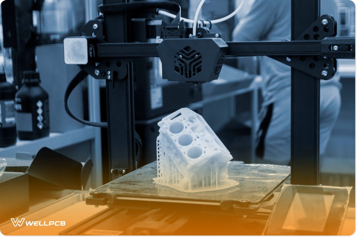
3D printing Prototype
3D printing gained popularity in the early 2010s, allowing enthusiasts, hobbyists, and professionals to print 3D structures directly from CAD designs. While convenient, 3D printing has never been suitable for large-scale productions—this remains true today.
Nevertheless, many players in the PCB manufacturing industry are exploring additive manufacturing for PCB prototyping. PCB production is typically a multi-phase process that involves diverse sets of machines and expertise.
Additive manufacturing allows manufacturers to 3D print a PCB in hours, or even minutes. This means the PCB prototype can be tested rapidly, saving time and money.
Ultimately, additive manufacturing appears to be the next evolution in rapid prototyping. Whether it’s capable of replacing PCB manufacturing entirely remains to be seen.
What Are the Benefits of Adopting Advanced PCB Manufacturing Technologies?
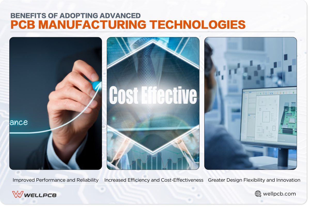
Benefits of Adopting Advanced PCB Manufacturing Technologies
Improved Performance and Reliability
Adopting advanced PCB manufacturing technologies can decrease costs and improve the quality, durability, and performance of your PCBs.
For example, innovations like glass weaving and advanced FR-4 materials have enabled the production of PCBs with lower dielectric values (DK).
This has, in turn, allowed manufacturers to minimize trace signal interference.
Increased Efficiency and Cost-Effectiveness
Processes such as LDI and additive manufacturing have facilitated rapid PCB prototyping. This is in contrast to traditional prototyping methods, which are often time-consuming, cumbersome, and prohibitively expensive.
Furthermore, as automation has reduced the number of human operators on the factory floor, injuries and errors occur less frequently.
It also makes it possible for manufacturers to mass produce PCBs cheaply, leading to lower costs and significantly higher output.
Advanced PCB manufacturing technologies have also facilitated environmentally friendly practices.
From less impactful waste disposal to greener materials, advanced manufacturing technology allows organizations to actively affirm their corporate social responsibility and reduce their environmental footprint.
Greater Design Flexibility and Innovation
Modern PCB manufacturing technology offers unparalleled design flexibility, allowing for greater customization and innovation.
Unlike older methods, which are limited in their design flexibility and customization potential, today’s computer-aided PCB design processes make it possible to experiment and test new ideas rapidly and at scale.
For instance, while traditional rigid PCBs are rectangular, advanced technology now allows for the mass production of PCBs with irregular shapes. This includes complex Rigid-Flex PCBs, which would otherwise be impossible to produce at scale.
What Industry Trends and Future Directions Can We Expect to See in PCB Manufacturing?
In the coming years, we can expect PCB manufacturers to increasingly embrace and offer additive printing services while AI and machine learning are positioned to advance 3D printing technology.
PCB manufacturers are also set to capitalize on industrial internet-of-things (IIoT) technology, leading to deeper automation, the ability to monitor multiple factory sites, and more sophisticated gathering of telemetry and other performance data.
Eco-friendliness will continue to be a key focus, with electronics makers gravitating towards manufacturers who prioritize biodegradable, non-toxic, and recycled materials. Technological advancements will also drive the adoption of zero-waste processes, making sustainable manufacturing more attainable.
To remain competitive, staying informed about technological advancements is crucial.
PCB technology is deeply connected with broader technological trends, so keeping up with general tech news is just as important as following PCB-specific updates.
For example, the rise of AI has driven demand for HDI technology in graphics cards.
Despite the slowdown in Moore’s Law, the trend towards miniaturization continues—all but guaranteeing continued demand for powerful, compact PCBs.
What Is Our Commitment to Innovation and Quality?
At WellPCB, we can reliably construct rigid PCBs with over 20 layers. We also offer SMT, through-hole, and custom mixed assemblies.
Our capabilities extend beyond rigid board fabrication and assembly—we can also build full flex-PCBs with up to 18 layers.
We operate state-of-the-art factories with a combined area of 15,000 square meters.
Our factories are equipped to support a wide host of reliability tests and checks, including probe tests, impedance tests, thermal shock tests, and hole resistance tests.
WellPCB offers a fully online prototyping service, allowing you to submit designs without having to speak to an operator directly.
We also cater to international customers and accept various file formats, including Gerber, .pcdbdoc, .cam, or .pcb files.
Simply send us your file, and we’ll perform a full design rule check and notify you of any issues.
Get Started with Our Advanced PCB Manufacturing Services
The technology used to manufacture your PCB significantly influences how it performs, both functionally and financially.
Early adopters tend to be most successful in the long run, and PCB manufacturing is no exception.
As the industry continues to evolve and we find innovative ways to refine and enhance the technology used to build PCBs, it’s essential to stay informed about new technologies and understand their impact.
WellPCB is committed to innovation and quality. We use the latest technology to deliver your orders on time, every time.
We’re more than just a service provider; we’re your partner in success. To start your PCB journey with us, use our online quote generator today.


