
Contents
- 1 What Is a Multilayer PCB?
- 2 Building Blocks: Key Materials in Multilayer PCBs
- 3 The Power of Many: Advantages of Multilayer PCBs
- 4 Real-World Applications: Where Multilayer PCBs Shine
- 5 Design Considerations for Multilayer PCBs
- 6 Manufacturing Challenges: Building Complex PCBs
- 7 Get Your Complex PCB Project Started!
What Is a Multilayer PCB?
A multilayer PCB is a printed circuit board with more than two layers pressed together, allowing it to accommodate more wiring, cores, conductive surfaces, and insulation.
While single-layer boards often have all components on one substrate layer, PCBs with multiple layers can contain anywhere from four to 50 copper layers, with components positioned on both the top and bottom layers.
For complex designs and increased functionality, your PCB production can benefit from the flexibility and capacity of multilayer PCBs, making them an ideal choice for advanced applications.
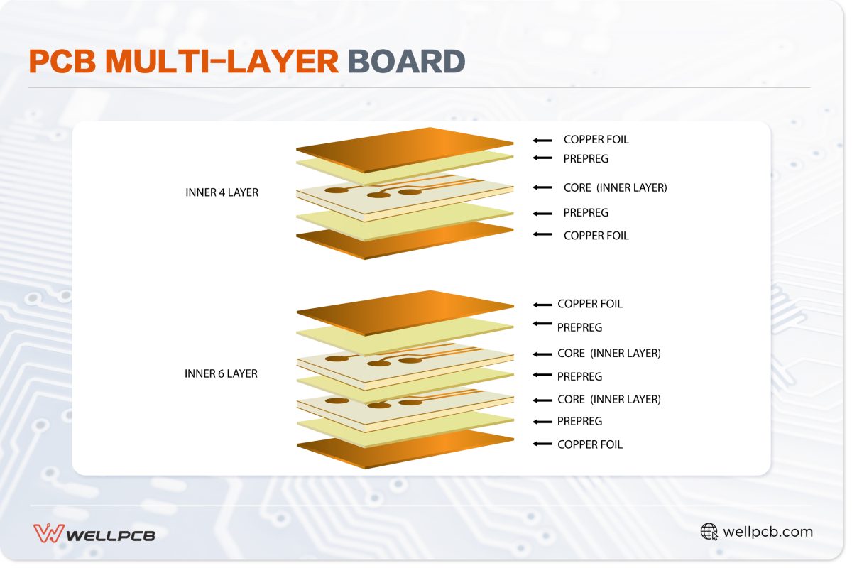
PCB multi-layer board
Why stack multiple conductive layers with insulating materials?
Manufacturers stack multiple layers with insulating materials in multilayer PCBs to increase current-carrying capacity.
There are typically three different layers in a stack: conductive, insulating, and plane layer.
- Conduction layers (signal layers): These contain copper traces that carry electrical signals to the board’s components.
- Insulation layers (dielectric layers): These prevent electrical shorts by providing insulation between the electrically active layers.
- Plane layers (ground and power planes): These are vital for electrical distribution on the power plane and grounding on the ground plane.
In a 4-layer PCB, the component side is on top, and the solder side is at the bottom, while the inner signal and inner plane layers are sandwiched between these.
Common Multilayer PCB Constructions
Here’s an interesting fact: multilayer PCBs can have up to 50 layers. That said, 4-, 6-, 8-, and 10-layer PCBs are most common.
4-layer PCB
4-layer PCB stackup | |
| 1 | Top layer |
| 2 | Prepreg material |
| 3 | First inner layer (power plane) |
| 4 | Core |
| 5 | 2nd inner layer (power plane) |
| 6 | Prepreg |
| 7 | Bottom layer |
The compact nature of the 4-layer PCB makes it more mechanically stable, so you can add more features and incorporate compact routing designs that reduce electromagnetic interference.
You can also design channels that allow for higher speeds and better signal integrity.
Due to its complexity, however, the 4-layer PCB is costly to design.
6-layer PCB
| 6-layer PCB stackup | |
| 1 | Top layer (component layer) |
| 2 | Prepreg material |
| 3 | Ground plane |
| 4 | Core |
| 5 | Route layer |
| 6 | Prepreg |
| 7 | Route layer |
| 8 | Core |
| 9 | Power plane |
| 10 | Prepreg |
| 11 | Bottom layer |
The 6-layer PCB has a more complex design. The power and ground planes provide power distribution and reduce signal noise, respectively, while the insulation layers allow you to place components close together with minimal risk of short circuits.
The additional layers offer better heat dissipation and reduced electromagnetic interference.
The distance between the ground and power planes makes 6-layer PCBs unsuitable for high-speed applications.
8-layer PCBs
| 8-layer PCB stackup | |
| 1 | Signal layer 1 |
| 2 | Prepreg |
| 3 | Ground plane |
| 4 | Core |
| 5 | Signal layer 2 |
| 6 | Prepreg |
| 7 | Power plane |
| 8 | Core |
| 9 | Ground plane |
| 10 | Prepreg |
| 11 | Signal layer 3 |
| 12 | Core |
| 13 | Power plane |
| 14 | Prepreg |
| 15 | Signal layer 4 |
While the 8-layer design is difficult to troubleshoot, given its complexity, the stack is ideal for high-density circuitry.
This is because the additional layers allow for better routing with enhanced signal clarity.
When stacked correctly, the 8 layers improve electromagnetic compatibility and provide room for more connections throughout the board.
10-layer PCB
| 10-layer PCB stackup | |
| 1 | Signal layer 1 |
| 2 | Ground plane |
| 3 | Signal layer 2 |
| 4 | Signal layer 3 |
| 5 | Power plane |
| 6 | Ground plane |
| 7 | Signal layer 4 |
| 8 | Signal layer 5 |
| 9 | Power plane |
| 10 | Signal layer 6 |
The 10-layer PCB stackup is ideal for applications that require high signal integrity and electromagnetic compatibility.
However, this setup is prone to slow or degrading performance when signal layers are added in the grounding and power plane slots.
As such, ensure layers are stacked correctly in the manufacturing process.
Building Blocks: Key Materials in Multilayer PCBs
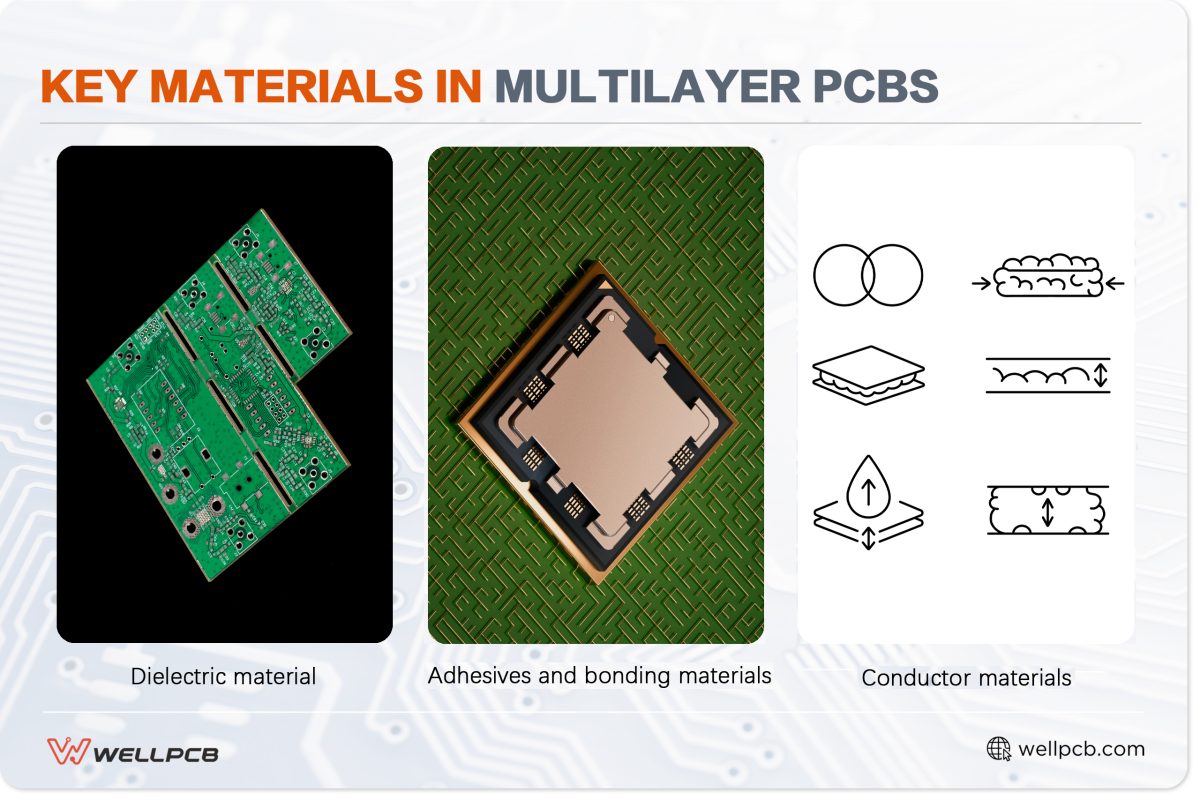
Key Materials in Multilayer PCBs
Multilayer PCBs may share a similar construction, but they differ in material. These materials influence their utility, longevity, and conductivity. That said, some factors remain consistent.
Dielectric material
Dielectric materials are poor electric conductors, making them ideal for insulation between copper layers to prevent electrical faults. Common dielectric materials include:
- FR-4: This fiberglass-reinforced epoxy is an inexpensive, flame-retardant material commonly used in PCBs. Its dielectric constant (DK) ranges from 3.8 to 4.8, making it suitable for most electrical applications. Additionally, the epoxy provides mechanical stability.
- Polyimide: Made from imide polymers, polyimides are mostly used in flex PCBs for applications that need enhanced flexibility and thermal stability at high temperatures. They have a low dielectric constant of 3.3 to 3.5, offering mechanically stable insulation.
- Ceramic: Ceramic is an alternative to polyimides and FR-4 for applications requiring rapid heat dissipation. While ceramic is more likely to break under pressure, it has a dielectric constant of approximately 9 to 10, depending on the type.
Conductor materials
Copper is the second most electrically conductive metal, with a conductivity of 58 MS/m at 20°C. Normal PCBs require standard copper thickness, ranging from 0.5 oz/sq ft to 1.0 oz/sq ft.
While manufacturers can use other metals, copper remains a popular choice for its stability in high-temperature and high-voltage applications.
Adhesives and bonding materials
While multilayer PCBs can be adhesives, most applications demand structural integrity. To that end, these are the most common adhesives used to bond multiple boards.
- Epoxy: Epoxy is a strong adhesive that bonds the substrate with the conductive material (copper). It’s often chosen for its structural and bonding stability in high-temperature environments.
- Acrylics: Acrylics are preferred for their thermal properties and minimal surface area, which is especially suitable for multilayer PCBs. They also have excellent dielectric properties, complementing the insulation used in PCB construction.
Material Matters: Properties to Consider
1. Electrical insulation (dielectric constant)
A material must have a low dielectric constant to be an effective insulator for multilayer PCB manufacturing. For example, polyimides are highly regarded as insulators as their dielectric constant is lower than FR-4.
2. Thermal conductivity (heat dissipation)
Multilayer PCBs often operate in complex equipment subject to high temperatures. As such, it’s essential to use materials that can dissipate heat quickly and evenly to ensure the longevity of internal components.
This is why materials such as epoxy, acrylics, and ceramics are preferred for high-powered applications.
3. Coefficient of thermal expansion (CTE)
Some PCBs may undergo significant expansion and contraction due to environmental changes. Therefore, selecting materials with matching CTE is crucial. The typical CTE value of multilayer PCBs is 16–18 ppm/°C.
A mismatch will result in solder fatigue or bridging, eventually causing short circuits.
The Power of Many: Advantages of Multilayer PCBs
Multilayer PCBs offer significant advantages in modern electronics, enabling complex and compact designs. Here are some key benefits:
- Multilayer PCBs can house up to 32 layers, making them a versatile option for applications that require extensive circuitry. This is achieved with a small footprint, ideal for compact units in household and industrial equipment.
- By using high-quality insulation and conductors, multilayer PCBs provide higher signal integrity and reduced EMI and radiation interference. This results in more accurate systems, even in high-power applications.
- Multilayer PCBs support advanced technological developments with complex designs while maintaining small and compact system sizes.
- Unlike single-layer PCBs, multilayer PCBs enhance a manufacturer’s ability to create multifunctional boards.
- As multilayer PCBs typically have one connection point, manufacturers can design complex systems with a single connection point. This helps avoid systems where single-layer boards are connected across many separate points.
Real-World Applications: Where Multilayer PCBs Shine

Multilayer PCBs Applications
Beyond consumer electronics, multilayer PCBs are vital in any application that requires pinpoint accuracy and effectiveness.
High-performance computing and servers
Multilayer PCBs are integral to high-performance computers and servers that demand high-heat dissipation and superior signal integrity.
Advanced medical devices
Devices such as MRI and X-ray machines operate in high-radiation or electromagnetic environments, while pacemakers need intricate wiring in a miniature casing.
Multilayer PCBs are essential to achieve accurate design in such advanced medical devices.
Telecommunication equipment and smartphones
From smartphones to network cell towers and repeaters, multilayer PCBs are crucial to minimize cross-talk and interference.
Aerospace and defense electronics
Aerospace and defense electronics such as radar equipment, target systems, and nuclear detectors need to operate in particularly extreme conditions.
Multilayer PCBs ensure accuracy and reliability in high-temperature, high-EMI, and highly charged environments.
Design Considerations for Multilayer PCBs
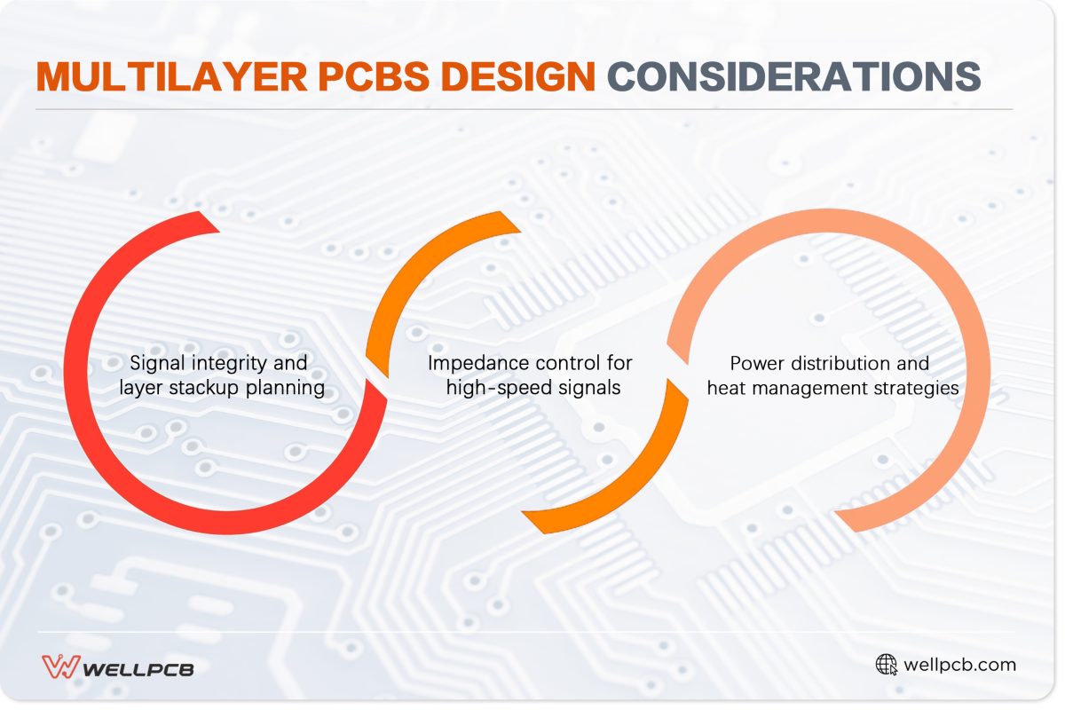
Signal integrity and layer stackup planning.
When designing multilayer PCBs, carefully stack layers to reduce cross-talk and interference.
The top and bottom of the stack should have solder masks, while the topmost layer and the layer above the bottom solder mask must be signal layers.
The GND planes and prepreg layers should follow the signal layers.
Impedance control for high-speed signals
Effective impedance control, achieved through tight stacking in the design and construction phase, ensures minimal signal loss and quick transmission of high-speed signals.
Power distribution and heat management strategies
You must strike a balance between copper thickness, layer spacing, and the choice of insulators and adhesives to optimize power distribution and heat dissipation, especially in high-energy applications.
Refer to your design worksheet to reduce assembly time and avoid adding unnecessary layers, which can increase costs.
Download our free guide to Design for Manufacturability (DFM) for Multilayer PCBs to learn how to streamline your PCB production process.
Manufacturing Challenges: Building Complex PCBs
Even with intricate designs and a robust assembling process, manufacturing multilayer PCBs presents several challenges.
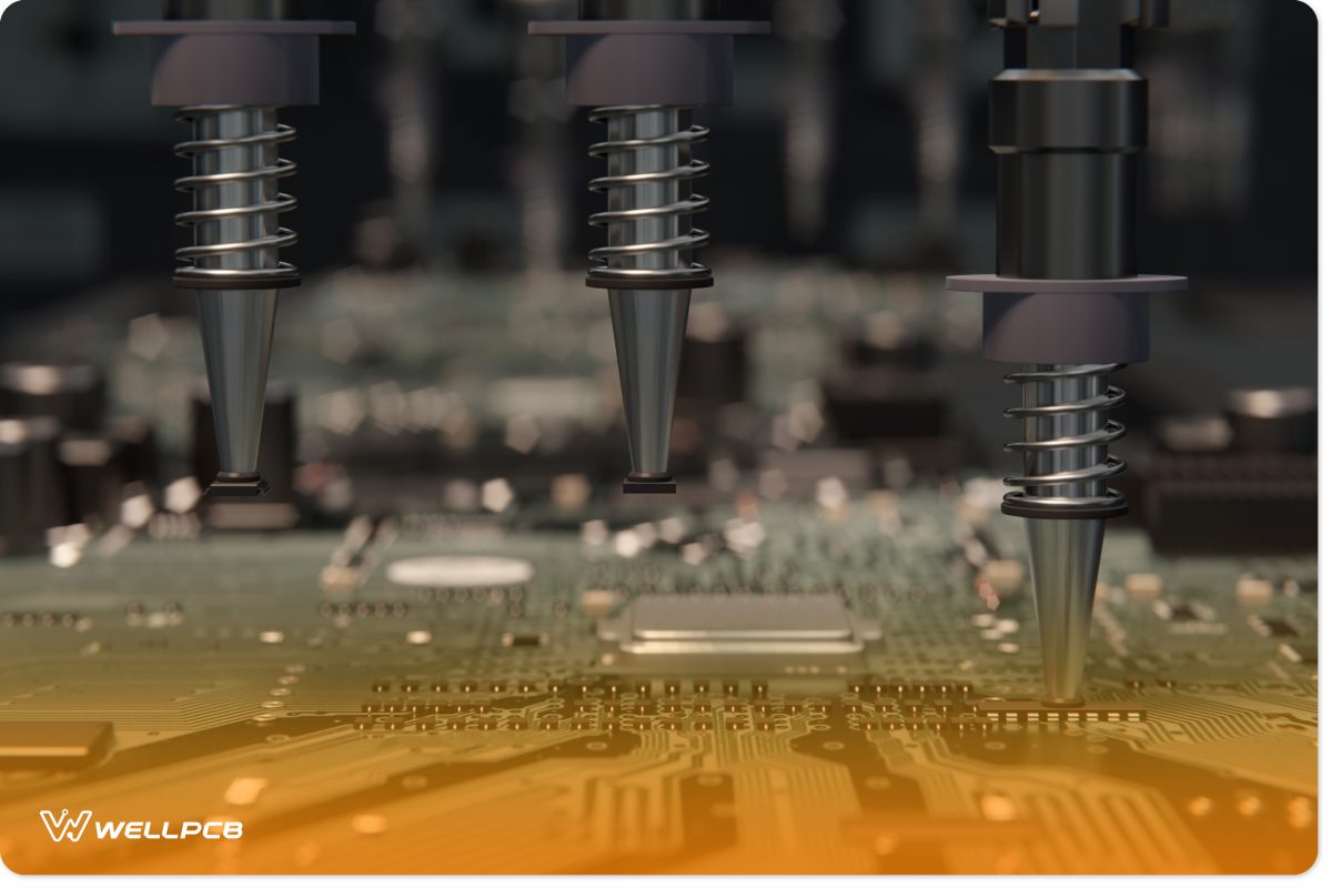
Pick and place technology in PCB assembly
Increased complexity and cost compared to simpler boards
Manufacturing multilayer boards require specialized machines, expertise, and rigorous testing. Any mishaps during manufacturing can lead to costly redesigns and reworks.
Even with a smooth manufacturing process, the costs of multilayer PCBs are inherently higher than those of single-layer or double-layer boards.
Potential for yield rate issues during fabrication
The yield rate is the percentage of usable boards from a complete fabrication run.
Challenges that might affect yield rate include unbalanced stacking, incorrect material selection, design and pressure control issues, and errors in Gerber file referencing.
Addressing these issues is essential to maintain a high yield rate and minimize waste.
Get Your Complex PCB Project Started!
Multilayer PCBs are an invaluable asset if you’re developing electrical systems for high-precision applications, as they offer reduced noise, better heat management, and more complex circuitry.
To achieve top performance, it’s crucial to outsource your PCB assembly needs to a reliable manufacturer.
WellPCB has a proven track record of working with reputable companies to produce accurate, high-quality, and complex multilayer PCBs.
We use automated processes to manage the entire process—from design to final testing and delivery logistics on a large scale.
Contact us today and request a free quote for your project.


