Contents [hide]
- 1 What Are The PCB Layers?
- 2 Layer Stack Up (Distinguish With PCB Layers)
- 3 PCB Layers Types
- 4 Multilayer PoolMultilayer
- 4.1 4.1 Multilayer PCBsMultilayer
- 4.2 4.2 Multilayer PoolMultilayer
- 4.3 4.3 Multilayer PoolMultilayer
- 4.4 4.4 Multilayer CircMultilayer
- 4.5 4.5 Advantages of Multilayer PCBsMultilayer
- 4.6 4.6 Disadvantages
- 4.7 4.7 How Multilayer PCBs Multilayer Single-Layer PCBs
- 4.8 4.8 Application
- 4.9 4.9 Multilayer Pool Multilayer
- 4.10 4.10 Multilayer Pool SMultilayer
- 4.11 4.11 Multilayer Pool CMultilayeracitor
- 5 PCB Layers Thickness
- 6 Pcb Layers Ordering
- 7 Conclusion
What Are The PCB Layers?
1.1 PCB Layers Definition
Printed Circuit Boards (PCBs) have different meanings depending on the message being relayed. PCB layers, also described as copper layers, are given a certain quantity and order.
The copper layers can be termed signal layers or just layers.
PCB layers are named out on their positioning and the functions they deliver. PCBs rank according to the number of copper layers.
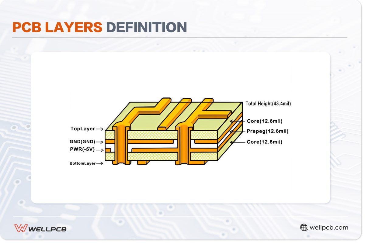
For example, boards with one or two layers can be termed 1-layer PCB or single-sided PCB and 2-sided layer PCB or simply double-sided PCB, respectively.
There are various types of PCB Layers, and the following are the common ones:
1. Mechanical Layer
2. Overlay / Silkscreen Layers
3. Routing Layers
4. Solder Mask Layers
5. Solder Paste Layers
6. Keep Out Layer
7. Ground Planes and Power Planes
8. Split Planes
Remember that not every PCB consists of all the layers enumerated above. Your design’s specifics determine the need for various layer types.
Single-layer boards usually comprise six-layer types.
These include a mechanical, a keep-out, a routing, an overlay, a solder mask, and a solder paste layer.
Multilayers of six layers plus a combination of other power plants, ground planes, and additional routing layers.
The most common boards are two-layer, four-layer, and six-layer PCBs; it is not unusual for PCBs to have more than 12 layers.
1.2 Mechanical Layer
While you may have several mechanical layers, you will still need at least one to construct your board. The most basic mechanical layer defines your board’s physical dimensions.
The mechanical layer is also known as Mechanical 1. The layer that the fabricator will use in cutting out the circuit board from their material.
Printed Circuit Boards can be as simple as just a single routing layer outlining your board’s physical dimensions or as complex as a board with many layers, including all the layers mentioned in this article.
On the other hand, when considered separately, every single layer has a particular and mere function. Understanding each layer’s purpose is essential because the moment you do so, PCB construction becomes extremely simple, regardless of how complicated the board is.
This framework can be either a simple rectangle or a complicated shape having curvy corners plus/or cut-outs.
Even though this is rare, more mechanical layers are included, specifying tooling specs and additional miscellaneous automatic information. However, most printed circuit boards do not require these extra mechanical layers.
Layer Stack Up (Distinguish With PCB Layers)
2.1 What Is Layer Stack Up?
A layer stack-up is the proper placement of a type of layer. PCBs are, in general, categorized into three:
- Single layers.
- Double layers.
- Multilayers.
The ayersterms describe the number of copper layers in a PCB. The multilayer Pmultilayers have more than two layers in the 4, 6, and 8 range.
In a multilayer, the multilayer bottom layers are known as the outer layers, while those in between are known as the inner layers.
The complexity of the manufacture of multilayer PCBmultilayerm quite costly compared to double and single-layer PCBs.
In layer stack up, there are a few things that you can put into consideration, and these include the following:
- The substrate material.
- The PCB layers order.
- The copper thickness.
Different circuit designs have different layer stack-ups that suit them appropriately. Layer stack-up is essential for the functioning of Printed Circuit Boards.
Different problems may arise when a layer stack-up is not well planned, and such include:
- Signals crosstalk.
- Coupling.
- Overshoot.
- Undershoot.
- Electromagnetic interferences.
- Signal dissipation.
It is vital to have a well-planned PCB layer stack-up to avoid the above problems and more. An efficient PCB layer stack-up can save a lot of time and money, which can go a long way in preventing issues arising from improper design.
In Layer Stackup other than the PCB layers order, substrate material, and copper thicknesses are also considered.
There are different layer stacks for different types of circuit designs. A well-planned PCB layer stack ensures the best performance of the PCB, such as decreasing electromagnetic interference, signal crosstalk, coupling, overshoot and undershoot, and signal dissipation.
The design to be completed and the qualified first time can significantly reduce costs and the design cycle time. It is possible if the signal integrity issues are eliminated before they arise.
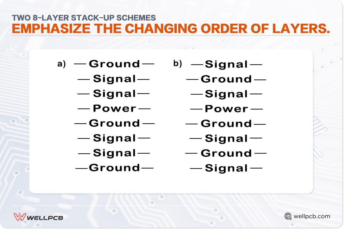
In Figure 1 below, two 8-layer stack-up schemes emphasize the changing order of layers.
Other than signal layers, power planes also play a vital role in successful product development.
The signals, either digital or analog, can route through microstrip lines or strip lines that reduce crosstalk and consequently improve signal integrity.
The low-frequency signals are routed on the inner layers, whereas the high-frequency signals are routed on the outer layers.
It is a good practice to place a ground plane layer adjacent to each signal layer; however, to reduce layer stack up and manufacturing cost, the ground layer is placed after each two signal layers. The power planes should also be adjacent to the ground planes that make the tight coupling.
In the case of multiple power supply rails, the power planes are split into more than one part.
The PCB thickness is usually 1.6mm, but it is challenging to maintain a 1.6mm thickness of more than 12 layers.
In Figure 1 below, two 8-layer stack-up schemes emphasize the changing order of layers.
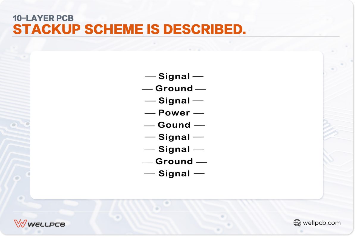
In Figure 2 10-layer PCB Stackup scheme is described.
2.2 Distinguishing PCB Layers From Layer Stack-Up
As much as these two terms may seem to mean the same thing, this is entirely not the case. As defined above, a layer stack-up is the proper placement of a type of layer.
On the other hand, PCB layers refer to copper layers given in a certain quantity and order. Whereas layer stack-up is concerned with the planning of layers, PCB layers are concerned with the amount and order of layers.
PCB Layers Types
3.1 1-Layer PCB
Often referred to as a single-layer PCB, the one-layer PCB is printed from one side; this implies that the PCB sheet is on one side together with a conductive material, while on the other side, electronic components are connected.
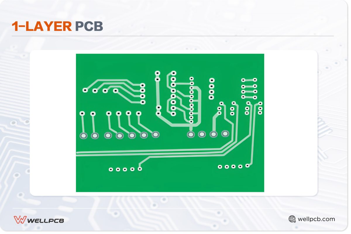
At first, all the PCBs were designed manually, but due to technological advancements, they can now be created using specialized software such as Eagle PCB. This is done using computers that have this program.
Single-layer PCBs come in different types. Some of them include the following:
• Flexible PCBs. These single-layer PCBs are made out of flexible material instead of rigid ones. Such materials that it can use in this case include plastics. The cost of production for this type of single-layer PCB is quite high, making it uneconomical.
• Rigid PCBs. These single-layer PCBs are made of rigid materials such as fiberglass. They are not flexible and thus cannot bend the circuit. They are commonly used in most devices, such as calculators, power supplies, etc.
• High-frequency PCBs. These single-layer PCBs are used in circuits requiring significantly high frequencies. In choosing the right material to be used for such PCBs, thermal expansion, water absorption, and dielectric loss are some of the factors that are considered
• Rigid-flex PCBs. These single-layer PCBs are made of a combination of plastic and fiberglass. The two materials are combined into a single layer, reducing the PCB’s size and weight.
• Aluminum-backed PCBs. These single-layer PCBs are made of aluminum. The design of this PCB is almost similar to that of the copper one, only that the difference occurs in the article that has been used.
Layer PCBs are quite simple, as you can see. However, let not their simplicity fool you for what they can achieve. They might be simple, but they produce much regarding working with complex devices. There are some functions that they perform, and some of them include the following:
- 1. They are used in radio and stereo equipment circuits.
- 2. They are used in digital cameras.
- 3. They are used in photocopy and printer machines.
- 4. They are used in digital calculators.
- 5. They are used in vending machines.
Single-layer PCBs have some advantages, for instance:
- Easy to come up with and design.
- Easy to install.
- Cost-effective.
- It is easily understandable.
- There are low probabilities of short-circuiting.
- More reliable and efficient.
3.2 2-Layers PCB
A two-layer PCB, or double-sided PCB, is mainly made of an FR-4 glass epoxy substrate laminated with thin copper film or layers on both sides. It is the simplest and most economical PCB to design.
A two-layer PCB can easily be manufactured by a professional PCB Prototyping factory (e.g., wellpcb.com) and made at home. Two-layer PCB has only the top and the bottom copper layers.
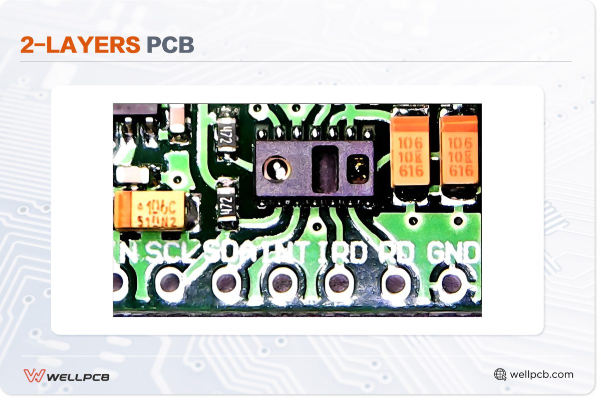
It is a simple design to develop, and it is also economical. This PCB design can easily be manufactured at home with the right software. It is mostly made by PCB prototyping companies.
The PCB layers in this design are mainly the signal layer, which forms the top layer, and the bottom layer, which comprises electrical components. All the components of a double-layer PCB are as follows:
- Trace.
- Pads.
- PCB layers include the silk, top, and bottom layers.
- Solder mask.
There are some places in which double layer PCB’s are used. Some of the areas of application include the following:
• In lighting. The double-layer PCBs are used in LED lights and thus the power they have.
• In medical devices. Double-layer PCBs are utilized in medical equipment such as pacemakers and CAT check machines.
• Automotive and aerospace industries. PCBs are in significant use in both the car and aviation industries. To be more precise, the double-sided PCB is used majorly in these two industries.
Double-layer PCBs come with a wide range of advantages. You can take a look at some of them below:
- They make the laying of tracks simpler.
- Permit higher thickness in segments.
- Offer expanded warmth scattering.
3.3 4-Layers PCB
A four-layer PCB has four copper layers. The top and bottom layers are the routing layers, while the two layers sandwiched between are the power and ground planes.
Between the Four-layer PCB Copper layers are the Core and the Prepreg. During manufacture, a laminate combines all these elements (sandwiches them) under high heat and pressure to ensure the whole stack-up is held together.
The four-layer PCB can contain through vias, blind vias, and buried vias. For a four-layer PCB, buried via can only be between the second and the third layer, and the blind vias can be between the top (first) and the second layer or between the bottom (fourth) and the third layer.
The typical stack-up for a four-layer board would be power & ground for the inner two layers and then the signals on the outer two layers.
One usually would route the two signal layers perpendicularly.
It’s not as critical if the layers are separated by power and ground, but if signals are on adjacent layers, it becomes more important to minimize crosstalk.
As for numbering, one usually goes from 1 to n, starting at the top and going down to the bottom. This is the only convention; you can do whatever you like, as you’ll provide the stack-up info when you send the files for production.
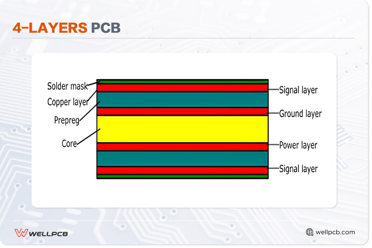
The cost of manufacturing a four-layer PCB can be quite useful if you have a manufacturing plant.
3.4 6-Layers PCB
The design that makes the six-layer PCB is immune and quiet. There are some reasons why the six-layer PCB is advantageous compared to the others. Some of the ideas include the following:
• The tracing between the third and first layers doesn’t require any special treatment.
• Every trace has proximity to the ground.

3.4.1 Reference Plane
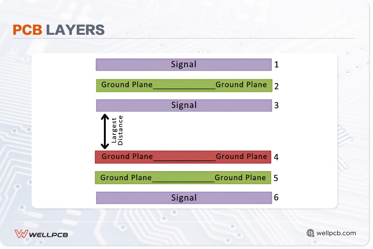
The reference plane is used for transferring the return current. In the four-layer design, layer one has a high-frequency return currency on the second layer, and the fourth layer has a high frequency on the third layer; hence, there is no difference with the six-layer PCB.
When the reference planes are moved closer to the routing or signal layers, you will have a cut-up on the loop area that determines the radiated emissions and the susceptibility in high frequency.
The following are some of the factors that make the six-layer stack work well.
1. The proximity to the ground by every trace.
2. The proximity of ground planes and power creates the planner capacitance.
3. tracing the third and first layers requires no special treatment.
4. The layer four reference plane is higher than the distance between it and layer 2.
3.4.2 The Common 6-Layer PCB Stack-Up Design
The best six-layer PCB design will require stitching to connect two ground planes in the PCB, which are supposed to return the current to the reference planes. Some say adding extra ground planes helps shield against emissions and immunity.
3.4.3 PCB Plane Cuts Kill EMC
Plane cuts can be devastating to the EMC in both emissions and susceptibility. Plane cuts or voids occur when the power or ground plane makes an unintentional or intentional cut through a given portion of a plane. And Plane cuts come in different sizes and shapes.
A current return path on the plane is a few thousand inches away, and in good designs, the trace runs adjacent to the plane, making the return current path nearby and forming the loop area relatively small.
When introducing a void in the copper plane layer, you must create a loop required for the trace to run across the voids and plane cuts. This makes the current loop area much more significant.
3.5 8-Layers PCB
An eight-layer board can add two more routing layers or improve EMC performance by adding two more planes.
The percentage increase in the cost of an eight-layer board over a six-layer board is less than the increase in going fro six layers, making it easier to justify the cost increase for improved EMC performance.
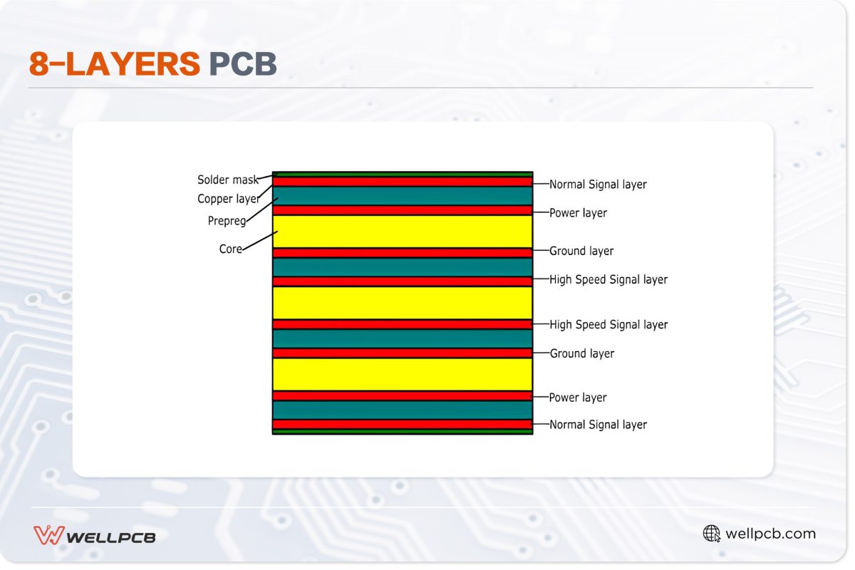
Therefore, most eight-layer boards consist of four wiring layers and four planes.
To make an Eight-layer PCB, you need alternating layers of the copper layer, prepreg, and core. The prepreg is the glue that firmly combines the Eight-layer PCB stack-up into a single board.
Following the rules to improve electromagnetic compatibility, a simple eight-layer PCB configuration would look as shown below. It is important to note that an Eight-Layer PCB can achieve high signal integrity compared to a 6-layer PCB and below.
You can choose the PCB stack-up design method according to the number of signal networks, device density, PIN density, signal frequency, and board size.
The higher the number of signal networks, the higher the device density; the higher the PIN density, the higher the signal.
Besides, ensuring each signal layer has its reference for good EMI performance is best.
Some advantages come with using an eight-layer PCB.
Some of the pros and benefits include the following:
• It reduces electromagnetic interference, which may lead to interruptions.
• It improves signal integrity.
3.6 Multilayer PCB
Multilayerayers PCB
It is merely a multilayer PCB multilayer 32 layers. The layers are put together to work as a single PCB. These PCB layers are advanced and thus require skills and precision.
Every PCB design starts with the software. For a 32-layer PCB, a stack-up contains many PCB layers. This is made possible by a machine that sandwiches the layers together.
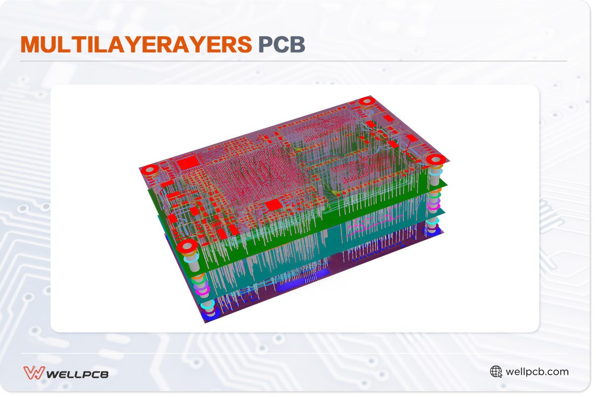
There are some reasons why you can choose to use the 32-layer PCB. Some of the ideas include the following:
• Used in aerospace systems.
• Used in the automotive field.
Technique Behind 32-Layer PCB
To manufacture a 32-layer PCB, a Stack-Up made up of multiple PCB layers is constructed.
It is made possible by sandwiching various double-layer PCBs with the help of an insulating fiber-epoxy layer between every two double-layer PCBs. This insulating material is also called prepreg.
It implies the basic building blocks of any multilayer PCB are multilayer-layer PCB.
With this two-sided PCB fabrication technique and more advanced machines to handle the increased complexity, fabrication of a 32-layer or even a 50-layer PCB is achievable.
32 Layer PCB Applications
Why do we need these 32 or 50 Layer PCBs? One of the obvious reasons is to efficiently embed all the necessary system electronics in one small-sized PCB.
Even though components assembly is dedicated to top and bottom layers, it is possible to have components between the Stack-up. The aerospace industry does an excellent job of making these complex PCB designs.
In any aerospace system, the target is to have as little or no electromagnetic emission as possible. Organizing a PCB during the design phase does a great job of arresting these emissions.
Each PCB layer is usually dedicated to a specific function that does not conflict with other layers. For example, the middle layers could be used as supply power planes, while the top and bottom layers are set aside for component placement.
3.6.2 Multilayer PCB
Multilayer PCBsMultilayernlimited number of conducting layers. Insulating layers then separate the layers. They are usually on the inside of double-sided boards, while the outer layers generally comprise single-sided boards.
The manufacturers of multilayer PCBsmultilayerand pressure to bond each of the PCB layers to form one PCB board. Any PCB with more than two layers can be classified as a multilayer PCB.
Its stack-up must be made so that the complete board meets the electrical signal and power needs and meets the mechanical strength requirements. Most professional PCB designs can exhibit around 15dB fewer emissions.
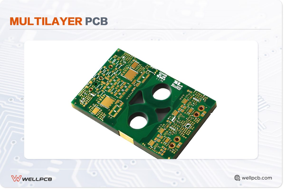
There are some reasons why you should consider using a multilayer PCB multilayering or double-sided PCB. Some of these reasons include the following:
- They result in high-quality and reliable products.
- They have a higher density of assembly.
- Increases functionality.
Precautions
When making a multilayer PCB, multilayer-plan the configuration of your PCB stack-up. A wrong PCB configuration may cause undesired electromagnetic interference and poor signal integrity.
Below are some of the essential things to consider about signals when making a multilayer PCB design.
- Consider the type of signals to be routed, e.g., different signal frequencies.
- Consider the signal rise and fall
- Sufficient return for the signal loop
Likely signal delay caused by permittivity – Possible cross-connection and overlap
Multilayer PoolMultilayer
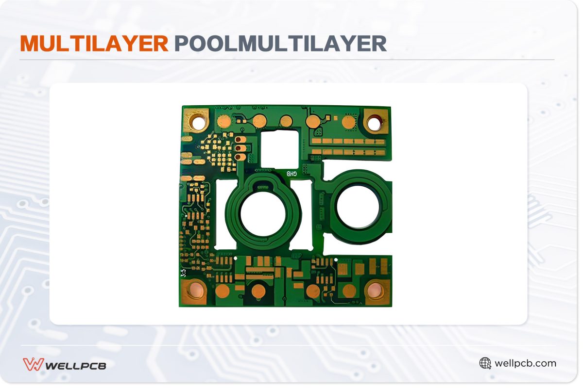
A circuit with more than two layers is known as a multilayer PCB.multilayer, this implies that the minimum number of PCB layers present for a multilayer PCB multilayerLaminating the materials together is not easy but is necessary for a multilayer pool.
A multilayer poolmultilayerve no air trapped between layers. Eagle PCB design software is necessary for its manufacture.
As usual, the process is complicated and starts with preparing a schematic diagram. The schematic is then edited using the Eagle software’s editor menu.
You may wonder why most PCB layers are even. It is important to note that it is more cost-effective to prepare even layers than odd ones. This is, therefore, the contributing reason for the layers being even.
4.1 Multilayer PCBsMultilayer
In making multilayer multilayer and prepreg materials are used to make the layers. Prepreg materials are those that are not cured, meaning that they are malleable.
Alternative materials of both prepreg and core are then laminated together under high temperatures and pressure, making the prepreg material. After cooling off, the layers are joined together, resulting in a hard and solid multilayer board.
Notice that the multilayer PCB multilayer a wide range of advantages that include:
- Increased flexibility
- Higher assembly density
- Controlled impedance features
- Small in size
- Have an EMI shielding
- It eliminates the need to interconnect harnesses, which reduces the overall weight
4.2 Multilayer PoolMultilayer
Multiple PCB-making processes involve using Eagle software to design PCBs. This complicated procedure starts with completing a Schematic diagram, edited through the editor menu in Eagle software.
4.3 Multilayer PoolMultilayer
After designing and drawing the schematic diagram, the next step is to work out the layout. This could be done by bringing the dimensions of your printed circuit board and uploading them to the software.
You can choose an appropriate grid to help each PCB layer overlap using the Eagle software. You could do this using a button that routes each layer separately per your needs.
Alternatively, you can create the multilayer poolmultilayerCB by auto-creating it using the Eagle software. However, if you choose this technique, you must cross-check the components, text, layers, and dimensions.
Using the check rule option to evaluate the final layout would be best.
4.4 Multilayer CircMultilayer
Multilayer prinMultilayert boards (PCBs) have become the core of the world’s electronics. They are the essential functions of components and wiring, making the new PCBs more advanced and sophisticated.
It gives the final users advanced flexible options and oddly shaped varieties to choose it.
‘PCBs for simple electronics consist of a single layer, while sophisticated PCBs such as those used in computer motherboards are multiple layers, called multilayer PCBs.
It is important to note that the advanced technology has allowed manufacturers to downsize PCBs significantly.
Multilayer PCBsMultilayermade with at least three copper foil layers. They appear like several single or double-sided PCBs glued with heat and protective insulation. The two layers are customarily placed on the surface side of the PCB.
Electrical connections in the layers are achieved through vias, such as buried vias and plating through the holes. This results in the generation of complex PCBs in varying sizes that are on the market.
Multilayer PCBsMultilayerovered during changes in electronics. Their continued use and function in modern electronics have made them more complex and sophisticated.
Initially, PCBs had problems, including crosstalk, capacitance, and noise. As a result, manufacturers had to devise specific constraints to limit the issues.
The design consideration meant it was prudent to design PCBs that would result in high-performance levels, hence the double-sided PCB. This understanding resulted in the discovery of multilayer PCBs.
It allowed for packing multilayer PCBsmultilayerl sizes to accommodate the ever-increasing electronics needs.
Modern PCBs have various layers, ranging from 4 to 12. The sheets come in even numbers to reduce issues such as warping, associated with an odd number of layers.
Also, producing an even number of layers is more cost-effective rather than building a different number.
Moreover, most modern devices, including smartphones and mobile devices, use PCBs with 12 sheets. Some manufacturers can manufacture PCBs with about 32 layers.
While manufacturing multilayer PCBsmultilayerintensive and expensive, they are becoming important in the modern world.
The reason for this is that they come with a host of benefits than what you would get with double or single-layer PCBs.
4.5 Advantages of Multilayer PCBsMultilayer
They are small in size, which is the most excellent feature of multilayer PCBsmultilayer smaller than single—or double-layer PCBs, resulting in a significant benefit to current trends.
They are more compact and robust and find many applica, smartphones, and tablets. The applications are lightweight in construction.
The smaller PCBs are less weighty since they don’t use multiple connectors that require them to be interlinked to double-layered and single PCBs. This increases the mobility of the devices in which applied.
• High quality. Creating a multilayer PCB multilayer proper planning and organization results in better-quality products than double- or single-layer PCBs. Also, these PCBs are more reliable.
• Increased durability. Multilayer PCBsMultilayere. They can withstand much weight and handle heat and pressure always applied to them during binding. They also have multiple insulation layers between the individual layers and a prepreg bonding agent that increases their durability.
• Highly flexible.PCB assemblers that use flexible construction techniques end up with flexible multilayer PCBs with highly desirable features, such as the ability to be applied in areas where flexing and bending will be required. However, it is important to note that the more layers used in a PCB, the less flexible it is.
• More powerful. Multilayer PCBs Multilayere many layers into a single PCB, enabling the board to be more connective. These properties allow them to achieve higher speed and capacity despite being small.
• Single connection point. Multilayer PCBs Multilayersingular units will always have just a single connection point, which is not the case when you use several single—or double-layered PCBs; this significantly benefits the electronic world as it helps to minimize size and weight.
4.6 Disadvantages
1. Although we have discussed the benefits of multilayer print multilayer boards extensively, it is critical to note that they have a few problems.
2. They are costly compared to single-layer PCBs because of the complicated manufacturing process and the extensive amount of time taken to construct them. This increases the labor cost which translates to high prices of PCBs.
3. They are more challenging to manufacture and require more time and advanced manufacturing techniques than single-layered PCBs because any small flaws could make them useless.
4. The supply is limited- because they need expensive machinery to manufacture, very few manufacturers can produce them, so their production is limited.
5. It requires extensive design and interconnection between the layers, and one should be able to mitigate impedance issues and crosstalk.
Any single mistake can lead to the board’s non-functioning.
6. Manufacturing the PCB requires plenty of time and person-hours, so delivering orders within the specified timeframes is sometimes difficult.
4.7 How Multilayer PCBs Multilayer Single-Layer PCBs
1. They are of high density and greater functionality because layering increases their capacity and speed.
2. They are small since adding layers increases their surface area, meaning you will have a higher-performing PCB than in a single-layer PCB.
3. They are light in weight since they require fewer connectors and can be used in complex electrical applications.
4. Multilayer PCBs have multilayered functionality compared to single layers and, despite their small size, offer great EMI shielding, controlled impedance, and other features.
4.8 Application
Multilayer PCBs Multilayered are preferred because they can be used across all technologies.
They are found in almost all electronics, including smartphones, microwaves, and other domestic consumer equipment.
Because they are small and have increased functionality, they are also used in smartwatches and mobile devices.
They find many applications in computer electronics, such as motherboards and servers. Their space-saving feature makes them easier to apply widely in the technology industry.
Multilayer PCBs Multilayeridely applied in telecommunication devices. They are used in GPS, signal transmission as well as in satellite applications.
Because they are durable, they can easily be in towers outdoors and on mobile devices.
Multilayer PCBs Multilayer in industries because they are small in size and durable.
Therefore, they are widely applied in industrial control and used in running machinery in industrial applications.
PCBs have also greatly benefited the medical field. They are found in equipment used in diagnosis and treatment.
They are small and lightweight, making them suitable for heart monitors, X-rays, medical testing devices, and CAT scan equipment.
Multilayer PCBs Greatly benefited the military. They are deployed in high-speed circuits and are highly utilized in military applications and devices that require increased movement.
PCBs have also significantly benefited the automotive industry, especially the electric car. They are used in GPS headlight switches and engine sensors.
They are small, durable, and heat-resistant, making them entirely applicable in the automobile environment.
4.9 Multilayer Pool Multilayer
The technology has allowed the production of quality boards and is considered key to military, communication, and other fields that rely on multilayer PCBs.
multilayerlogy enables manufacturers to fabricate PCBs from materials such as flex, Teflon, and polyimide, allowing them to fulfill their PCB needs.
4.10 Multilayer Pool SMultilayer
PCBs play a vital role in manufacturing computer networking devices, such as multilayer switches; multilayers provide extra functions, including routing capability.
The switch can prioritize packets and implement QoS-differentiated services in hardware.
4.11 Multilayer Pool CMultilayeracitor
They are popularly referred to as MLCCs and are used as building blocks in modern electronics. MLCCs comprise more than 30% of the components in the hybrid circuit module.
They consist of a monolithic ceramic block with electrodes that appear on the surface end of the ceramic block, which forms the contact made by having a burnt-in metallic layer.
Types
MLCCs come in different kinds, including tolerance, capacitance, dielectric, case size, etc. Their values vary but most commonly range from 10 nF to 1µF.
Also, their voltage rating ranges from 16V to 100V.
As technology advances, more and more multilayer PCBs amultilayerd. These PCBs are finding many applications in both the research industry and science.
They are used in security appliances, alarm systems, and fiber optic sensors.
They are also used in weather analysis equipment and atomic accelerators. Multilayer PCBs Multilayerlightweight, compact, and save on space.
PCB Layers Thickness
Different PCB layers have different thicknesses depending on where they will be applied. For instance:
- 11-layer boards can be of 20 by 14 dimensions unless given additional specifications.
- Six layer boards are produced on a 0.031, 0.040, 0.047, 0.062 and 0.125 inches thickness.
- The 8- and 10-layer boards have 0.062, 0.093, and 0.125 inches thicknesses.
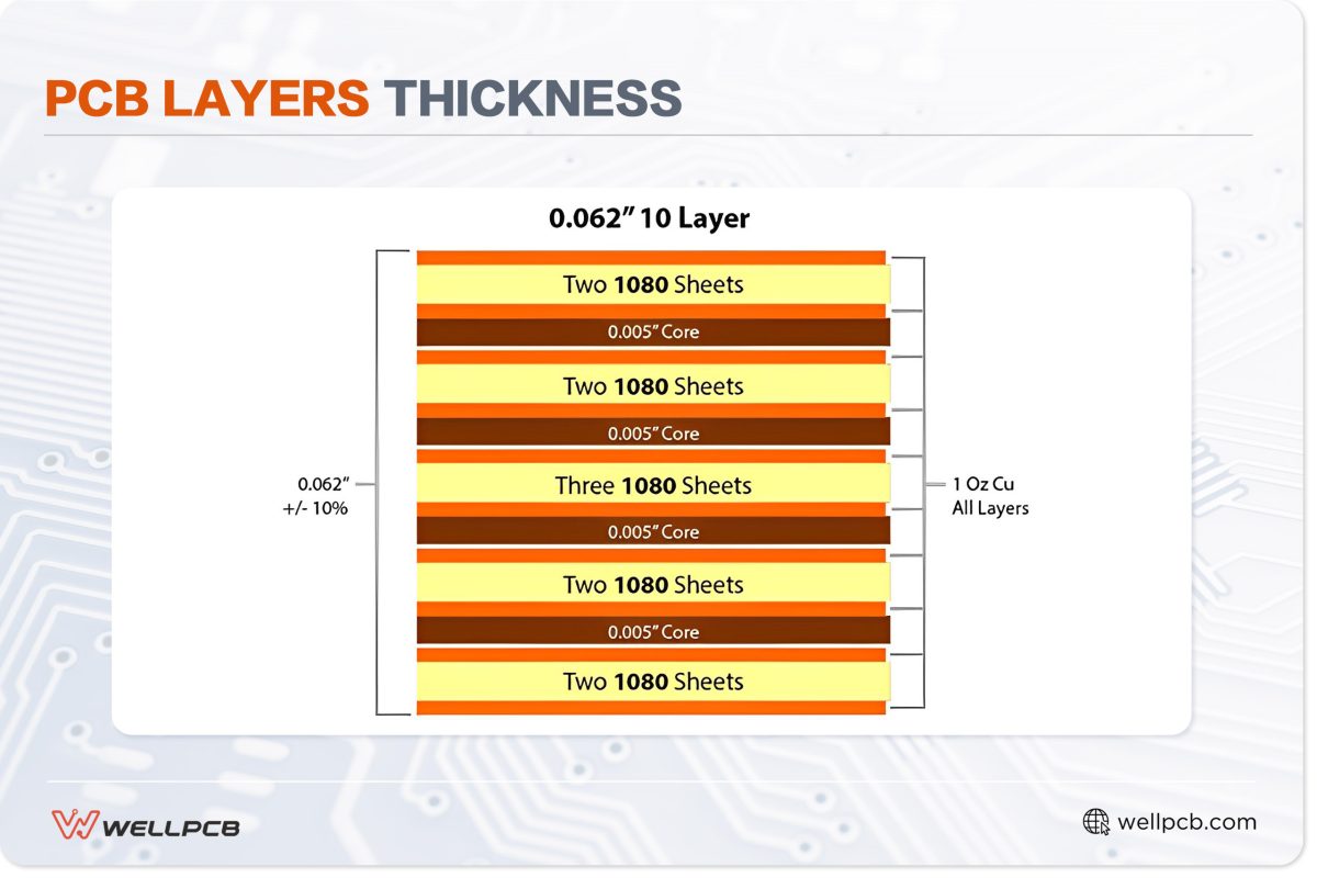
The standard pooling thickness for multilayer PCBs is multilayer. The standard measurement is not the actual measurement for all the multilayer PCBs but the multilayer as a reference in their construction.
Pcb Layers Ordering
PCB layers are arranged in order. The process of organizing these layers can be as follows:
• Choosing the initial number of layers. Here, you will select the PCB layers that suit your needs. One or two layers can be quite useful if you are doing home prototyping. Four layers of PCBs are simple or rather cheap boards.
Six-layer PCBs are cheap and abundant. Eight-layer PCBs are cost-effective, while 12-layer PCBs are ideal for heavy industry boards or boards with many tracks.
• Starting the layout
• Here, you will begin with the top and bottom signal layers. Depending on the design that you are using, the two top and bottom signals would be just enough unless you have too many connections requiring inner signal layers.
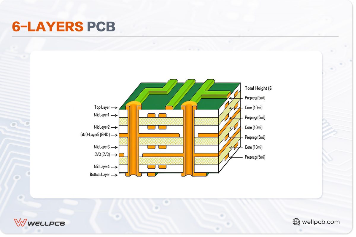
There are some options that you can use to order your PCB layers. The following are some of the most common ones:
- Four layers stack up.
- Six layers stack up.
- Eight-layer stack up.
- Ten layers stack up.
- Twelve layers stack up with two additional signal layers.
- 12-layer stack up with 4 GNDs.
You can make a quote of the type of PCB you would want here: https://www.wellpcb.com/pcb-quote.
Conclusion
As you have seen, PCB layers make up different designs of Printed Circuit Boards for various appliances. The sheets vary depending on where you want to use the PCBs.
The single- and double-sided layers are cheaper to construct but do not perform the complex operations that the multilayer PCBs canmultilayerer PCBs areMultilayerore advanced machines and electronics.
Multilayer PCBs areMultilayerof three or more PCB layers formed of copper, among other materials. In case of any inquiries and issues, you can contact us through the following:
• sales@wellpcb.net


