Contents
What is OSP?
Organic Solderability Preservative (OSP) is an environmentally friendly and cost-effective organic layer. This organic layer can bond to copper surfaces through absorption. Interestingly, the layer offers the same qualities you get from other surface finishes.
However, OSP offers a more permanent solution for dealing with exposed copper. And, since the organic layer can’t interact with other surfaces, you’ll have an easier time soldering and removing flux from your OSP PCB.
We used the first instance of OSP formulas in the 1970s. But, those formulas were weak and only worked for lower devices. However, the more advanced OSP formulas have improved durability and can handle higher device operations.
Main Materials of OSP
OSP formulas use rosin, azoles, and active resin as the primary materials. The rosin material works like a coating that you can apply to a flux treatment.
Interestingly, azoles are water-based compounds with heterocyclic nitrogen. These compounds are helpful because they have fantastic synergies with copper surfaces. This synergy is what starts the absorption process and creates a protective film.
The protective film you make depends on the type of azole compound used. There are three types of azoles: benzotriazoles, benzimidazoles, and imidazoles. Using benzotriazoles would make a thin film, while those made from imidazoles are thick.
Lastly, you’ll need to rinse your surface with acid or other solutions. As a result, it would help topographically enhance your character before adding the OSP finish.
Manufacturing Process of OSP
The process for manufacturing OSP has three stages: oil removal, micro-corrosion, and film formation.
Stage 1: Oil Removal
Removing all the contaminants and oil is crucial if you want a high-quality protective film. Otherwise, you’ll end up with an uneven film.
Luckily, there are ways you can avoid uneven films. First, you’ll need to control the concentration of your oil removal solution. Then, inspect the process to see if it’s okay.
If you notice that the effects of your oil removal are poor, you’ll need to replace it fast with chemicals specifically for this purpose.
Step 2: Micro-corrosion
Micro-corrosion aims to create a natural copper surface. Also, it directly influences how fast your OSP forms. Additionally, it’s vital to control the micro-corrosion thickness if you want a stable film thickness.
Also, the acceptable range for maintaining micro-corrosion is between 1.0um to 1.5um. Once you have your maintenance values, it’s easy to measure the micro-corrosion rate.
Step 3: Film Formation
It’s crucial to use DI washing before and after forming your film. Also, you must limit the solution’s PH between 4.0 and 7.0. Otherwise, you’ll contaminate the solution for film formation.
Here’s where the OSP process gets tricky. First, you need to control the film’s thickness so it doesn’t affect your welding performance. The ideal thickness can be anywhere between 0.2um and 0.5um.
Note: the thinner your film is, the fewer OSP advantages you’ll get. For instance, you may get lesser thermal shock capacity or oxidation protection. Also, remember to use DI washing after forming your film.
Advantages of OSP
OSP’s main selling point is how easy it is to process and its low-cost requirements. While these two advantages make OSP pretty popular, its other benefits make it an excellent surface finish:
1. OSP uses water-based compounds, making the surface finishing process environmentally friendly. Thus, we can classify OSP PCBs as green electronic products.
2. OSP PCBs have a long shelf life. Hence, they hardly succumb to wear and tear.
3. They have an easy manufacturing process. Also, these boards require little maintenance, and you can easily rework them if necessary.

PCB Manufacturing
4. It’s not expensive or complicated to repair an OSP surface coating when damaged.
5. You don’t need solder mask ink on an OSP board. And it’s because most OSP simple chemical compounds can handle the task. However, there are exceptional cases where some chemicals will need a little solder mask ink.
6. OSP boards can dish out exceptional performance, especially in the soldering area.
Disadvantages of OSP
Although OSP surface finishes are one of the best, it has some disadvantages. These downsides include:
1. OSP finishes require extra care because of their susceptibility.
2. You can’t use plated through holes with an OSP-coated PCB.
3. It’s also hard to measure the thickness of an OSP PCB.
Other Factors to Consider Before Using an OSP PCB
Here are some factors you should consider to avoid substantial PCB damage.
Storing your OSP PCB
OSP PCBs can last for extended periods, but that’s only when you treat them with care. Preservatives made from OSP are powerful but thin. Hence, you’ll need extra care when transporting and operating these boards.
Otherwise, the preservatives will break and make your board useless. Also, you must avoid storing OSP PCBs in high or humid temperatures for long periods. Or else it would increase the possibilities of oxidation and reduce solderability.
However, you can avoid all these by sticking to the following storage principles:
1. Ensure you use vacuum packages with desiccants and humidity display cards to store your boards. If you’re stacking multiple boards, place release cards between them to avoid friction.
2. Avoid exposing your OSP PCBs to direct sunlight. For instance, an ideal storage environment should have 30 to 70% relative humidity, 15 to 300C temperature, and a maximum of 12 months of storage time.
Possible Problems after Soldering OSP Boards

PCB Soldering
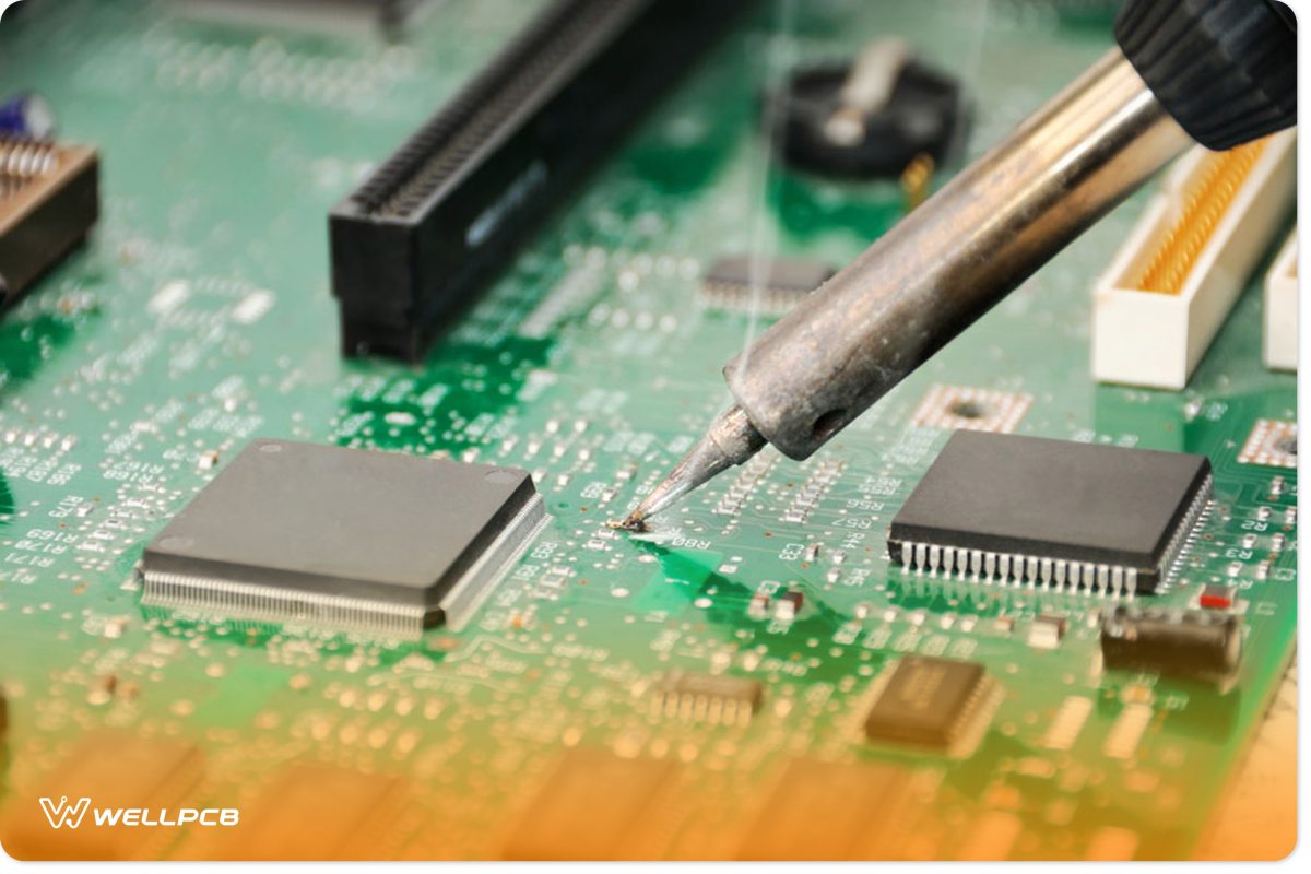
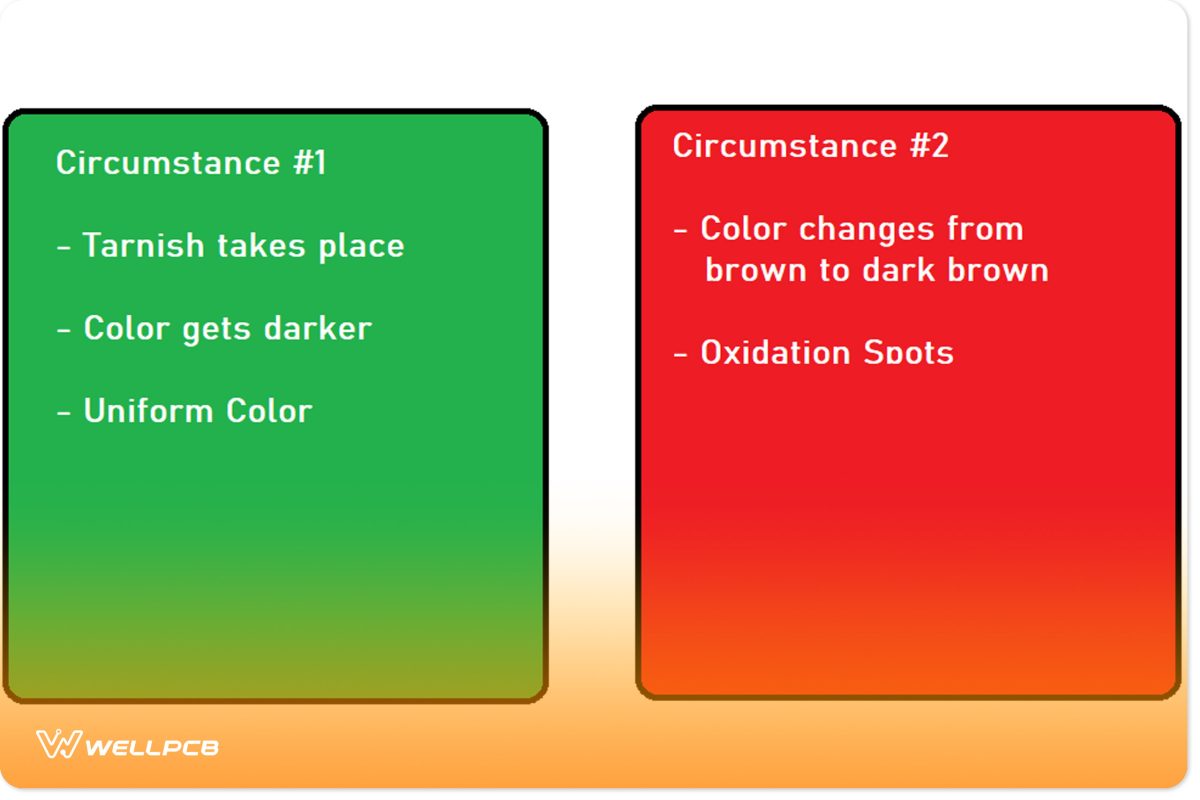
It’s normal for the color of an OSP board to change after soldering. However, two circumstances show if it’s a positive outcome or a problem.
Note: Color change could result from preservative thickness, abnormal contaminants, soldering time, or micro-etching quantity.

Soldering Circumstances
Circumstance one is an acceptable situation. It usually happens when flux eliminates oxidations, which protects the soldering performance.
But circumstance two is not a good situation. And it means you have an OSP board with compromised integrity. As a result, flux won’t eliminate oxidations, and soldering performance will be reduced.
Luckily, there are specific actions you can take to avoid circumstance two. These actions include:
1. Always control your OSP thickness by keeping it within specific limits.
2. Also, ensure you limit your micro-etching process to particular ranges.
3. Lastly, eliminate all contaminants during PCB fabrication to avoid solderability issues.
Which Is Better: ENIG, OSP, or HASL
ENIG (Electroless Nickel/Immersion Gold) is the best flat surface and lead-free surface finish globally. It offers excellent features and durability. But it’s expensive and hard to find compared to other surface finish options.
On the other hand, OSP offers a less expensive alternative without sacrificing performance. It’s also lead-free and can last for extended periods.
Lastly, HASL (Hot Air Solder Leveling) is an excellent choice if you don’t mind an option that contains lead. Also, HASL stresses circuit boards with high layers, which causes reliability issues.
Rounding Up

PCB
OSP is the go-to if you want an excellent surface finish that’s cheap and effective. It also bonds excellently with copper and won’t interact with other surfaces.
OSP PCBs may have weak preservatives, but they won’t pose a problem if you can manage them properly.
Do you want to manufacture an OSP PCB? Please feel free to contact us.


