
Contents
What Is a Printed Circuit Board?
A printed circuit board is a thin board that organizes and connects electrical components in nearly all electronic devices.
It’s made of insulating material and has electrical pathways etched or printed onto the board surface. These pathways connect components like resistors, capacitors, and microchips, allowing them to work together.
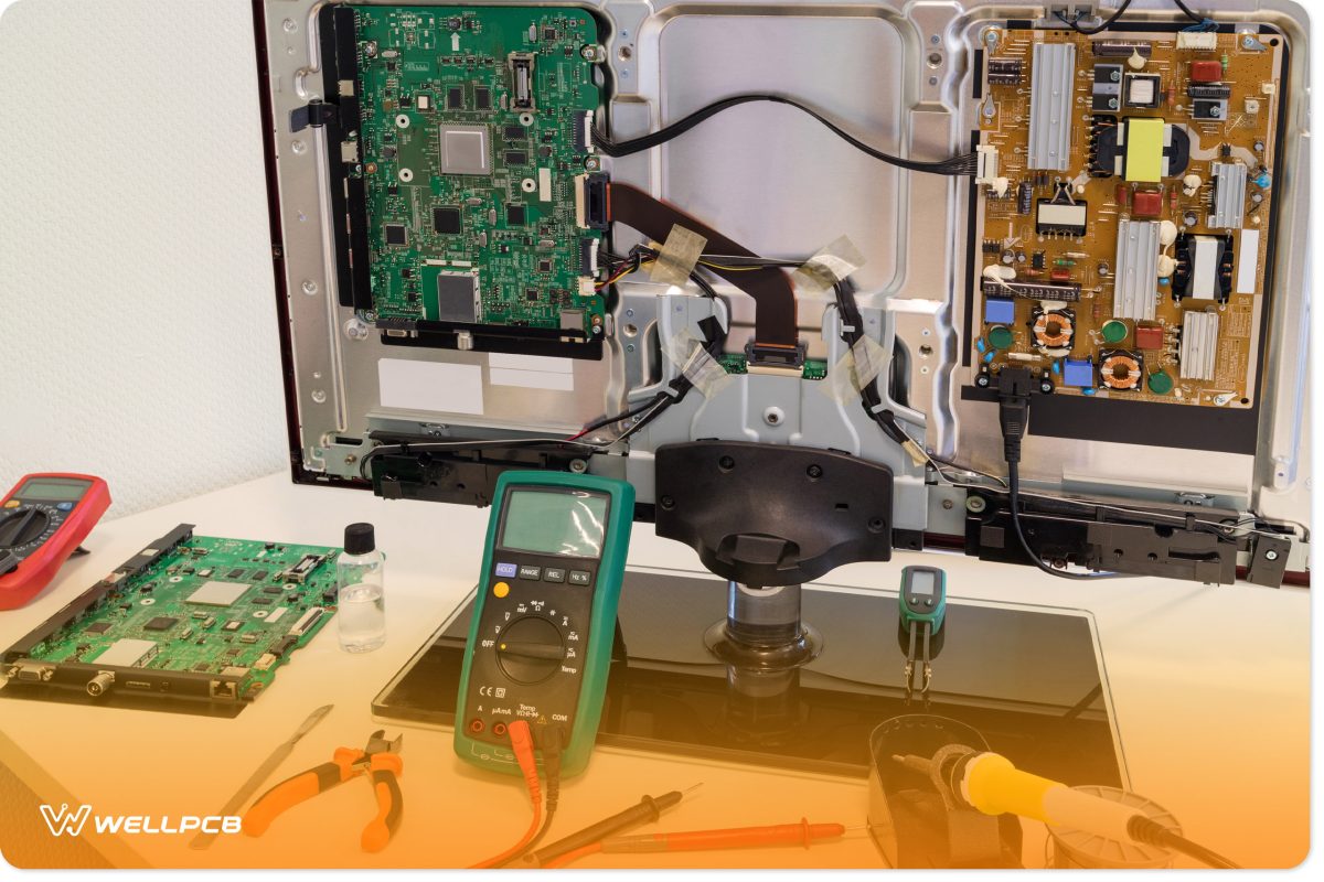
Consider your television. It consists of many smaller electronic components and has a power cable. The collaborative effort of these components makes your TV work the way it does.
However, these components must have a way to connect, communicate with each other, and power up. This is where PCBs enter the chat!
Essentially, a PCB acts like a roadmap, guiding electrical current where it needs to go to make electronic devices function.
Part of the reason why modern printed circuit boards are revolutionary is because they provide a compressed medium to connect components.
Without PCBs, electronics manufacturers would still be using printed wiring boards (PWBs)—which consisted of large tangles of cables and wires—to achieve the same purpose.
PCBs haven’t completely negated the need for wires and cables. We still use them to connect different PCBs together.
However, PCBs have improved the manufacturability of electronics, made them more reliable, and have allowed us to make more compact devices (miniaturization).
How Does a PCB Work?
A modern, single-sided printed circuit board consists of a conductive layer sandwiched between two dielectric (insulating) layers.
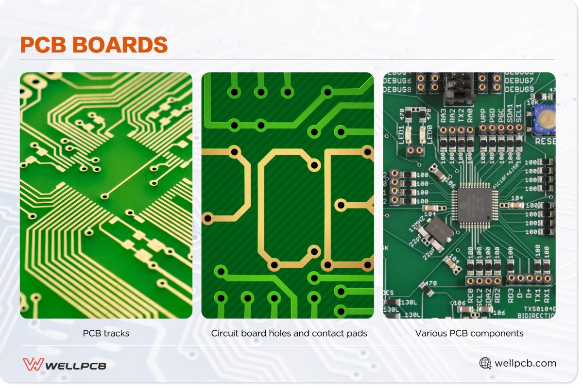
Manufacturers can also etch the conductive layer onto the dielectric layers (substrate). In this case, we refer to them as traces or tracks.
The conductive layer is usually composed of copper traces since it’s a reliable and inexpensive conductive material. It essentially acts as the embedded wires (circuitry) of the PCB.
The dielectric layers of the PCB usually consist of a tough fiberglass material. Its purpose is to provide a uniform structure for the PCB while insulating and protecting the conductive copper layer.
Before we consider a PCB to be a completed printed circuit board assembly (PCBA), it must have electronic components mounted (or soldered) onto it.
Pads and through-holes allow us to attach electronics to the PCB. Vias (thin, conductive paths) enable us to form electric connections between the various layers of the PCB and, ultimately, the electronic components.
Accurate component placement is critical for the board to function correctly. You need to position resistors, capacitors, microchips, and connectors in their designated spots, as they impact the electronic device’s electrical connections, signal integrity, and overall performance.
Different Types of PCBs
PCBs are categorized according to the number of conductive layers they have. There are three types:
- Single-layer PCBs: These consist of a single conductive layer, making them simple and cost-effective. However, because they’re limited by the number of components they can accommodate, they’re not ideal for high-power and complex applications.
- Double-sided/double-layer PCBs: These consist of two conductive copper layers separated by a dielectric lamina. Although you can mount electronic components on both sides of the boards, they’re more costly to manufacture and less compact than their single-sided counterparts.
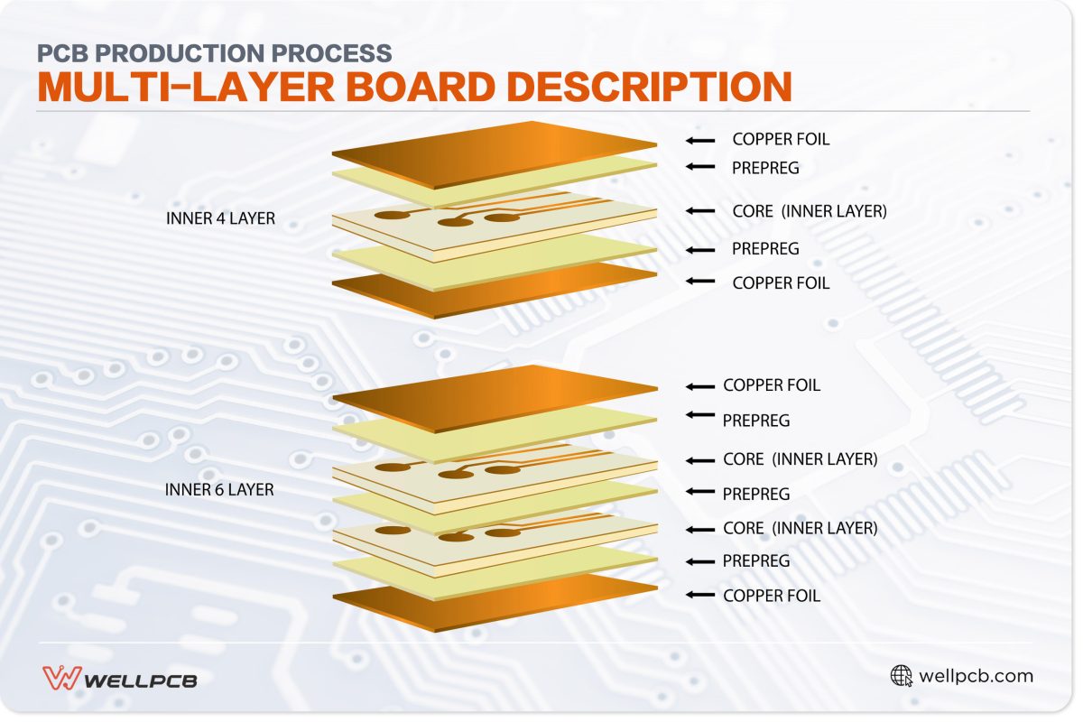
- Multi-layer PCBs: These comprise three or more conductive layers insulated by a dielectric lamina. Because they reduce electrical noise and crosstalk, manufacturers use them to construct high-current PCBs. They share many of the shortcomings of double-layer PCBs but to a greater extent.
Benefits of Using PCBs
Before the advent of PCBs, electronic device manufacturers used chassis-mounted wired point-to-point connections.
But, devices that use point-to-point connections—especially large, complex networks—are more difficult to manufacture, maintain, troubleshoot, and repair.

Although techniques such as wire-wrapping are still applied today, they’re mainly used by hobbyists. PCBs address and overcome many of the shortcomings of these techniques, improving:
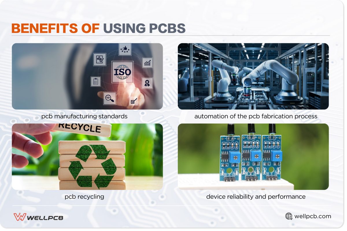
- Manufacturing standards: It’s easier to develop and maintain a manufacturing standard for a modern PCB. Replicating the structure and design of a PCB is also straightforward.
- Automation of the fabrication process: Set standards make automating the fabrication process more feasible than it is for point-to-point connections. As a result, we’ve been able to reliably and effectively mass-produce PCBs and the electronic devices they bring to life.
- PCB recycling: While many PCBs and PCBAs are built for specific applications, they can sometimes be repurposed and used in other devices. Historically, PCBs have been notoriously difficult to recycle. However, this will soon change as manufacturers adopt new techniques and technologies. PCBs will be easier to recycle and reuse than old wired technology, making them more cost-effective than prior technologies.
Common Applications of PCBs

Different types of PCBs are more suited to certain applications than others. For instance, single-layer PCBs work perfectly well for calculators, older mobile phones, simple handheld gaming devices, and educational purposes.
However, they have limited space for board components and are susceptible to cross-talk and interference, so they’re unsuitable for high-power applications.
Consequently, applications such as modern smartphones, tablets, modems, and more advanced communications devices use double-layer PCBs.
Highly complex applications such as robust military hardware, medical equipment and devices, and industrial machinery use multi-layer PCBs.
Regardless of the type or application, the fundamental purpose of a PCB is to control the flow of electricity within these devices.
For example, your smartphone contains multiple sensors, antennae, readers, and a screen, all powered by a lithium-ion battery.
The battery power runs through the PCB, where the components divert, transform, and distribute it to all the connected devices.
The circuit board also acts as a passage for signals, sending them back and forth between these devices.
All these minute transactions and processes make your smartphone work the way it does.
PCBs in Action: A Deeper Dive
High-density interconnect (HDI) PCBs are often considered a fourth type (type 4) of PCB. They’re essentially more advanced multilayer PCBs with at least four layers.
HDI PCBs are suitable for applications that require a lot of connections. They have a high connection pad density with more precise spacing and lines. Also, they use microvias through capture pads to form more intricate connections between layers.
We use HDI PCBs in advanced machinery, particularly those used in industrial automation. They’re also suitable for medical equipment, supercomputers, 3D printers, and image processors.
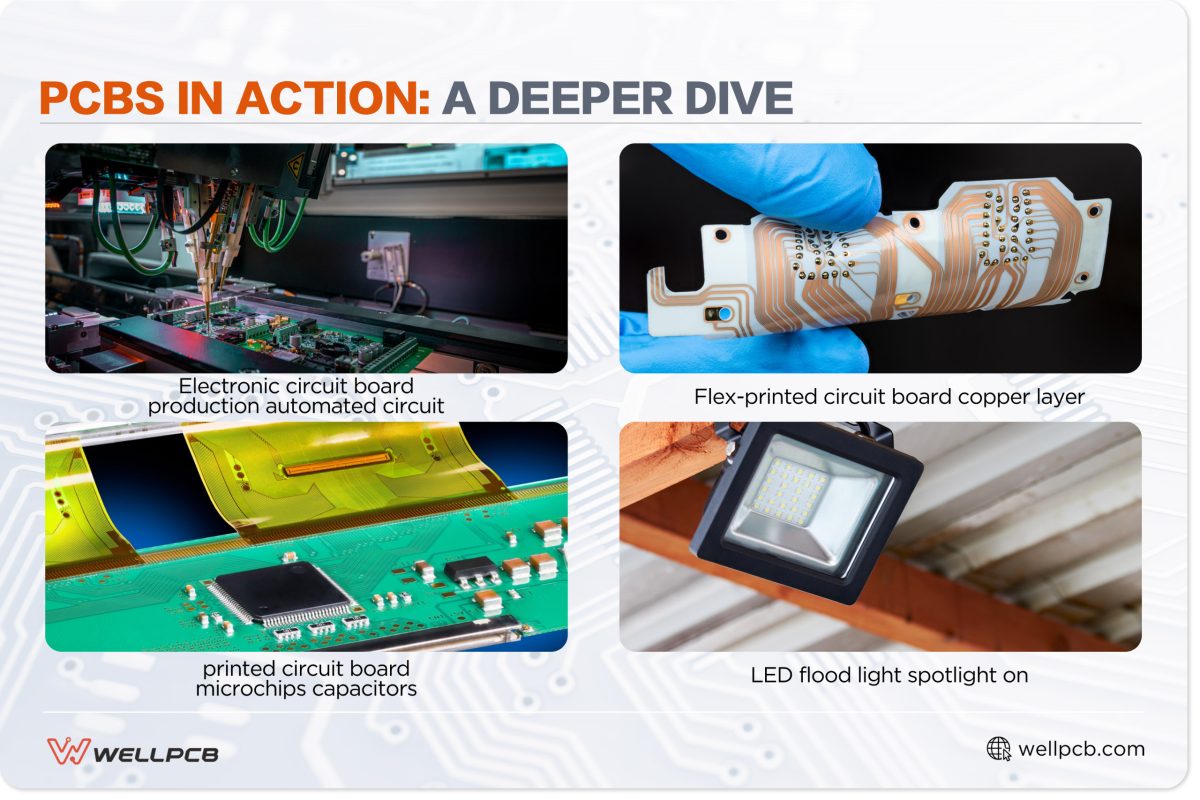
In fact, much of the automated machinery used in PCB fabrication and assembly uses HDI PCBs.
The PCBs we’ve explored so far are primarily rigid PCBs. This means they consist of solid material you aren’t meant to bend.
Flexible PCBs (FPCBs) also exist. They consist of flexible materials that can be bent, making them ideal for compact designs.
As with rigid PCBs, they come in single-layer, double-layer, and multi-layer formats.
You can also find PCBs that use a combination of rigid and flexible base materials. We refer to these as rigid-flex PCBs.
These typically consist of flex boards connected to one or more rigid boards. You can usually find them in military and medical equipment.
Aluminum-backed PCBs are another type of PCB used in high-power applications. These circuit boards feature an aluminum plate or layer that aids heat dissipation.
The aluminum also gives them a high level of rigidity, making them ideal for applications that require high mechanical tolerance, such as power supplies and flood lights (LEDs).
Ready To Design Your Own PCB?
PCBs can be complicated constructs. Even designing them as a hobbyist is time-consuming.
As you create more advanced designs, you need to be able to identify the type of materials to use for your PCB.
For instance, you must select the type and color of silkscreen and solder mask.
Besides those, you also need to consider the manufacturing scheme and how to attach the components.
Here, you have two options: through-hole technology (THT) and surface mount technology (SMT).
The former involves inserting component leads into drilled holes on the PCB, while the latter involves directly mounting components on the surface of the PCB.
Visit our blog to learn more about the PCB design and manufacturing process.
Get Your PCBs Manufactured!
Since we know that PCBs can be complicated and intricate devices, WellPCB is committed to helping you get the most from your PCB layout.
We perform comprehensive Design Rule Checks to ensure the feasibility and integrity of your printed circuit board design.
We accept four file types: Gerber, .pcb, .pcbdoc, and .cam. Once validated and confirmed, we can begin prototyping or mass-producing your PCBs in our modern, 15,000-square-foot factories.
Why wait? Get a quote for your next PCB project today!


