
Contents
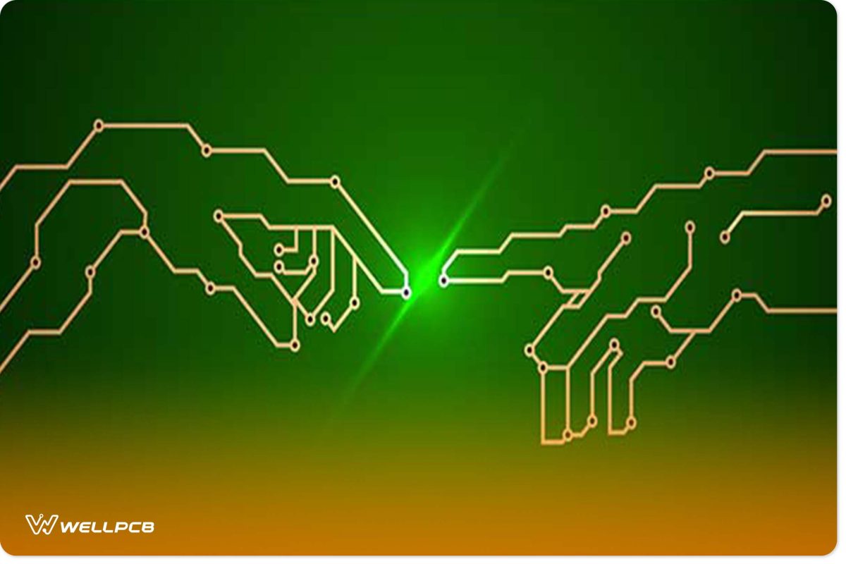
What is PCB Art?
In a nutshell, “PCB Art” is a generic term that defines an attempt to create an artistic impression on a Printed Circuit Board (PCB). Such an image might be drawn during the Gerber design or cut through during manufacturing.
Let’s take the example of a wristwatch’s PCB. I bet we all know of the good old rectangular-shaped watch PCBs with strictly utilitarian squire-shaped drawings linking ICs and other electronic components. Now, compare that simple ancient design with the modern age of complicated boards with intricate and artistically drawn interconnection of parts and multiple layers.
Assuming we eventually manufactured the two PCBs (the old PCB without art and the new PCB with art) and deployed them in the watch market, won’t both designs show you the time? Of course, they would. Then why should you spend a fortune to add art on PCBs?Is it worth it?

The design does not matter a lot when you need to attain a practical goal, but it does matter when you need to sell or impress. As an individual, you might need to examine the designs that would look impressive, the ones that would perform better, and the technology improved. Often, such design considerations would influence higher market sales among several competitors. PCB art is commonly used to attain these goals of PCB manufacturing.
Top Three Simple But Beautiful PCB Art Ideas
Idea 1: “Birth of Adam” Contact Pads
These contact pads that resemble fingers are simple to design but beautiful to behold. You can utilize them when designing any generic PCB.
Idea 2: The Christmas Tree Art

Christmas is often a season of sending gifts. In modern times, most people consider electronics as gifts for festive seasons like Christmas. So, if you are thinking of producing electronics that can be sold as gifts, why can’t you add Christmas tree art? Not necessarily to make it worthwhile but just because you can.
Idea 3:The “Brainy” PCB Art

When designing consumer electronics, you might consider setting a different design for the microprocessor. A better idea would be to utilize a “brain” art to differentiate the processor from other components. It would look more appealing and would become easier to troubleshoot.
How to Do A PCB Art in Design
The skill of PCB art designing originated from within the engineers of technologically advanced electronic manufacturers. In modern days, this skill has found its way into the DIY (Do-It-Yourself) hobbyist manufacturers’ crafts pack. It is currently applied in the production of the simplest to the most advanced PCB productions.PCB arts are everywhere. You will meet them hidden in the electric shaver while you take a morning shower, or you will put them on as smartwatches when going to work.
In today’s market, electronic companies (especially phones) and creative PCB art designers often team up to design and produce complex small-sized PCBs with initially unimaginable functionalities.
Besides the consumer electronics audience, PCB arts have also extended into DIY projects like auxiliary jewelry and gifts.
Top Five Software Application Tools of PCB Art Designing
Designing is sometimes a challenging task. But you don’t have to begin it in the wrong way; that’s why you need some designing tools.
When designing a PCB, you will need a proper software application for creating the Gerber or vector file(s) for your PCB. Thanks to the internet, you will often find hundreds of such tools available for download. And that variety of choice is sometimes a “blessed curse,” as you might have a hard time distinguishing the best from the rest. This section will briefly explore some popular designing tools, especially the “free-to-all” applications, to aid you in getting started. Let’s begin with.
The Eagle Design Tool
Eagle is a PCB designing software product owned by Autodesk. It is not an open-source application. Then again, it is the most popular software for designing PCBs. Eagle has the following outstanding features:
Key Features
- A multicolored schematic PCB editor
- Several libraries are available for reusing
- Enhanced error detectors
It stands out for its vast supportive community and broad features of the design. Then again, this software is costly to acquire and maintain. Because of its cost, it is commendable for commercial usage.
KiCad EDA
KiCad EDA is an Open-Source PCB designing software. It has been developed to suit both commercial and learning uses. Some of its outstanding features include:
Key Features
- It supports up to 32 copper layers
- It gives on-design error prompts that alert you when you while designing
- Has an easy-to-use footprint editor
KiCad uses a 3D viewer for easy viewing of layers and error checking. It is also a free-to-use cross-platform tool. Both beginners and professional users are likely to find it helpful.
EasyEDA
EasyEDA creates a different paradigm for PCB design by making its tool an online-based PCB designing tool. I (personally) find it intriguing when creating designs that demand collaborative efforts, especially when designing or working with physically unreachable engineers.
EasyEDA is a better tool for DIY projects because it’s cheap, demands fewer resources, and performs essential tasks. It is recommended for its vast support of designs from other designing tools, ease of use, and open-source nature. Besides, you don’t have to install it; you will quickly get going if you can open it on a browser.
Proteus
Just like Eagle, Proteus is a vendor-off-the-shelf PCB designing software application developed and owned by LabCenter Electronics. It is a powerful tool with over 800 microcontroller options to choose from when designing your circuit.
Then again, Proteus is costly to acquire. It is an excellent tool for professional use. But if you are working on a tight budget as a hobbyist, feel welcome to skip it.
TinyCAD
Now, TinyCAD is the “plain and simple” PCB designing tool. This product of Sourceforge is free to use, but its design is highly simplified. I do recommend it highly when drawing schematics.
It is an excellent tool for experimentation and a perfect tool for hobbyist DIY projects. Nevertheless, it lacks the right testing tools for professional usage.
NOTE
PCB arts demand art ideas. After choosing an ideal tool, you will need to carefully consider the concept behind the art you will develop and whether it will be easy and affordable to produce it. Once you establish your idea, the process of designing it is simple. It often follows the steps below.
Steps to Designing a PCB Artwork
Step 1: All PCB Artwork Designs Begin with Schematics
Before you set out to develop any PCB Art, it is recommendable to lay out the circuit schematic of the PCB you intend to produce. A schematic diagram will enable you to establish the number of components you need for a PCB with their connections. The PCB designing tools (described above) can then import all the necessary details, wires, and footprints to ease your process of designing.
When drawing schematic diagrams, you need to be keen and import the components independently and selectively modify their parameters (e.g., resistance, capacitance, etc.). An error made in the schematic is likely to cost the final product of a PCB.
Tip
At this point, you should (not necessarily) strive to create your connections and components placement to represent the art you intend to make vividly.
Step 2: PCB Design Optimization
Here is where you will isolate the different interacting modules of your PCB project and how they are interrelated. You will need to prune any unnecessary components, unwarranted interconnection, and any unnecessary cost.
You will need to begin aligning your Schematic components into the desired art you intend to produce at this phase.
Tip
An important PCB design guideline to follow when optimizing and drawing the PCB art at this step is to keep the power source/unit of your PCB as close to your circuit’s modules as you can.
Step 3: Make TheConceptual Shape(s) Physical
Once you complete the process of creating the schematic, it will be necessary to eventually carve out the actual shape and design of your PCB. Here, you will only need to know the dimensions of your design (from the schematic), then use image designing software to design a shape or a layer for your PCB.
All the authentic art on a PCB should be saved in SVG format to enable secure processing on other image-processing applications.
Tips
Consider using specialized image processing software tools like Photoshop (if you can) and then export them for use into your PCB designing tool.
Drill holes and add copper artistic layering additions to ease and make designs appealing. However, be keen not to affect a design’s physical connections.
Add a solder mask on the added copper artistic effects or copper writings to insulate the connections from the art.
PCB Art Designing Considerations
Size
Ensure to use universally accepted size calibrations like “in” or “mm” when designing the shape.
User Interface & Peripheral Locations
Peripheral ports like power pins, audio jacks, LED indicators, or customization buttons should be carefully thought of while designing to minimize production errors. To attain a better user experience, you might consider compromising some parts of your art to achieve a better user experience, especially for consumer electronics.
PCB Layers
The thickness of a layer determines the amount of current that can pass through a layer without damaging the coating. The standard layer thickness is measured in ounces (oz.). Thicker layers have lesser resistivity and can move more current than thinner layers.
PCB Traces
For most professionally designed PCBs, edges or bends of connections are done at 45 degrees rather than 90 degrees. The main reason for this phenomenon is that at 45 degrees, fewer signals are reflected as opposed to a reflection of signals at 90 degrees.
Connections Routing
When you finish designing, you can either implement the routing manually or automatically. In the case of a simple circuit, an automatic routing could do best. However, if the connection is vast and complicated, do consider aligning the routing manually.
Testing and “Design Rule Checking”
A “Design Rule Check” is a popular accessory incorporated in most PCB designing tools to aid in design error checking. This tool allows you to set specific requirements (e.g., layer thickness) that should apply to your entire PCB, and the designing software checks the design as a whole and then highlights the parts that do not conform.
Layer Substrate:
Depending on the purpose of your art, you might need to use a white substrate and draw the art using copper masked with an insulating layer. A white translucent substrate enables you to view connections and art hidden within the layers.
Notably, lower-layer graphics will appear pale than upper-layer graphics.
Art precision and measurements:
The measurements of the layers should be equal, and the design of graphics should be coherent. To attain better pictures, ensure to use of similar units of quantization for length and thickness.

Conclusion
PCB Artworks give an artistic life to a lifeless PCB. With better investment in PCB art designs, you can improve the quality of your PCBs and increase their performance. In return, you will attain higher market sales and retain authenticity among your customer base.
As you might have noted, a good PCB art is an asset; a poorly designed one can become the most significant liability. That’s why you need professional guidance in the design and manufacturing of your PCBs. At WellPCB, we have built our reputation on producing quality PCBs with precision in the printing art. Do consider requesting a quotation of your PCBs (with art), and we will take you through the few steps of actualizing them.


