
Contents
- 1 1. Consider the Sizing of Your PCB Trace
- 2 2. Maximize Efficiency With Decoupling Capacitor Placement
- 3 3. Group Components Efficiently
- 4 4. High-Frequency Loops Should Be As Small as Possible
- 5 5. Reduce Resistance and Inductance With Kelvin Connection Placements
- 6 6. Use Your PCB’s Surface Area as a Heatsink To Provide Thermal Relief
- 7 7. Consider How To Lower Shock and Other Safety Hazards
- 8 8. Use a Qualified PCB Assembly and Manufacturing Service
1. Consider the Sizing of Your PCB Trace
Copper traces in PCBs, like regular wires, have a resistance that depends on their thickness.
Thinner traces result in higher resistance, which leads to greater voltage drop and power dissipation, ultimately generating heat. Excessive heat can damage the substrate, harm components, or, in extreme cases, even start a fire.
Additionally, voltage drop caused by high resistance may lead to underperformance or malfunction, as components may not receive sufficient power.
Since resistance is a physical property, managing it requires careful consideration of trace length, width, and thickness to ensure smooth current flow. This is especially crucial for specialized designs, including and rigid-flex PCBs, where optimized trace management is essential for balancing flexibility with performance.
These factors are interrelated, with the resistance of a trace being calculated using the formula:
Thickness is particularly important and is measured in ounces. One ounce of copper is the thickness of the metal if one ounce is spread evenly over a 1 square foot area. This turns out to be 0.0014 inches.
Most PCBs use 1 or 2 ounces of copper in their traces, but high-power traces may require up to 6 ounces.
We recommend using a trace width calculator to find the ideal width and thickness for your board. Just make sure that the temperature rise doesn’t exceed 5°C.
Thickness has its limitations, however. Fine features, such as traces routed from a chip, can only be so thick due to their proximity to each other.
When designing multilayer PCBs, remember that the inner layers have more material to dissipate heat through.
As such, they should be thicker or have efficient cooling mechanisms, like vias.
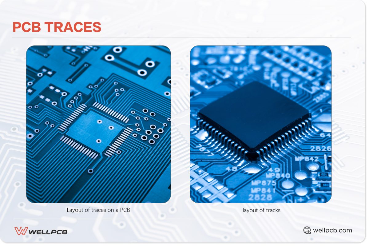
2. Maximize Efficiency With Decoupling Capacitor Placement
Decoupling capacitors are critical in PCBs as they absorb noise from one part of the circuit, preventing it from affecting other sections.
However, their placement is just as important as their function.
To maximize their noise absorption efficiency, decoupling capacitors should be placed as close as possible to the power and ground pins of integrated circuits.
Placing them too far away introduces stray inductance, reducing their effectiveness.
Another important factor to consider is the ground plane connection.
Using multiple vias to connect the decoupling capacitor to the ground helps minimize inductance and reduce noise even further.
3. Group Components Efficiently
Optimizing the placement and grouping of PCB components involves balancing many factors.
For instance, separating analog and digital components helps reduce noise, maintain signal integrity, and maximize reliability.
High-powered components usually generate a lot of heat, so they should be separated from any that are heat-sensitive, such as electrolytic capacitors or thermocouples.
These hot components should not be grouped together, however, as they can create intense hotspots that risk damaging the board.
ICs or components with high pin counts should be positioned centrally on the board in order to simplify routing.
When creating the PCB pattern, remember to keep noise-sensitive traces away from high-frequency signal lines.
Placing these too close together creates signal coupling, which can disrupt the circuit board’s performance.
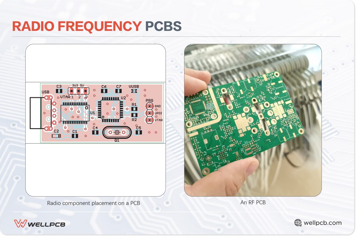
4. High-Frequency Loops Should Be As Small as Possible
High-frequency loops create significant inductance and resistance in the circuit, so they should be as small as possible.
Small loops offer several additional benefits, such as:
- Reducing voltage spikes
- Lowering the risk of inductive coupling from external sources or broadcasting signals to other areas (as with antennas)
Op-amp loops should also be small to prevent noise coupling in the circuit. However, even small loops create some inductance, so placing them above ground planes will keep inductance levels as low as possible.
5. Reduce Resistance and Inductance With Kelvin Connection Placements
Kelvin connections are a 4-wire connection method used for precise measurements of parameters like voltage and resistance.
These wires are connected directly at the points of contact, such as the resistor pads, rather than along the PCB traces.
This approach ensures accurate measurements by avoiding the inductance and resistance introduced by the traces.
As such, using Kelvin connections to link to other components reduces the resistance and inductance values associated with transmission lines.
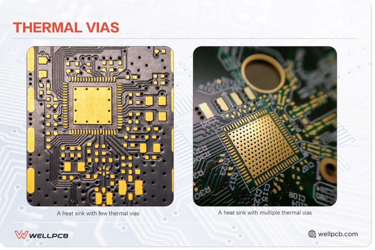
6. Use Your PCB’s Surface Area as a Heatsink To Provide Thermal Relief
Extra copper on the PCB surface can act as a heatsink, providing thermal relief to heat-sensitive components and improving their efficiency.
This is especially important when dealing with surface-mount components, which have limited air circulation around them.
Most high-power SMT component datasheets, such as those for MOSFETs, diodes, and voltage regulators, include guidelines on how to use PCB surface area as a heatsink.
However, for large surface-mount devices, such as ICs, thermal vias are necessary to provide low thermal resistance paths to the other side of the board.
These vias are plated-through holes that can work independently and when paired with heat sinks layered on the surface where the chip sits.
The more vias you have, the faster the heat will dissipate.
7. Consider How To Lower Shock and Other Safety Hazards
To avoid exposing the board and its components to shock and other safety hazards, consider the following techniques:
- Leave enough space between the copper fills/traces and mounting holes.
- Separate heat-sensitive components from heat-generating components.
- Use thermal pads, vias, and heat sinks to provide efficient cooling.
- Isolate low- and high-voltage circuits using optocouplers and transformers.
- Use TVS diodes to suppress voltage surges and prevent electric shock.
- Add multiple vias around mounting holes to reinforce the board against mechanical stress and vibrations.
8. Use a Qualified PCB Assembly and Manufacturing Service
Lastly, partnering with a qualified PCB assembly and manufacturing service provider is crucial for optimizing your design for manufacturing and assembly (DFM and DFA).
During the design process, manufacturers can provide valuable guidance and insight based on their capabilities.
For example, they can advise on the minimum trace thickness they can produce to meet the requirements of your circuit.
Ultimately, the best partner will be a qualified and capable fabrication house that adheres to international standards and maintains high-quality manufacturing.
At WellPCB, we’ve set high standards of quality and customer satisfaction, aiming for positive evaluation of at least 98% before our PCBs are shipped.
This has made our client list grow exponentially, with the expertise and state-of-the-art equipment to match.
We currently produce over 10,000 PCBs monthly, including rigid, flexible, and rigid-flex types, in single, double, and multilayer layouts.
With our experience and capabilities, we can help you design efficient PCBs using the tips outlined above.
Simply send us your design files (Gerber, pcb, pcbdoc, or cam) or project details, and we’ll guide you through the process.
Contact us today to get started!


