
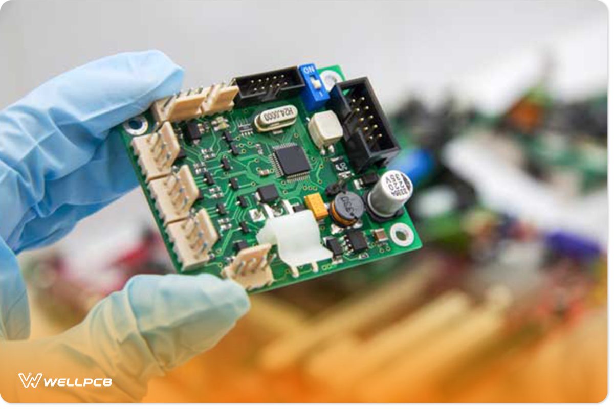
Contents
Solder Paste Inspection (SPI) Machine
SPI machines play a crucial role in inspecting and fabricating printed circuit boards. They conduct precise and rapid testing of soldering paste on the board, ensuring high-quality paste application and identifying any potential PCB fabrication faults. Through visual inspection, SPI systems monitor this paste for common errors.
By closely examining the PCB surface, these machines can detect flaws such as scratches, nodules, and pigments. Equipped with multiple light sources and HD cameras, they capture detailed images of the solder paste on the board. SPI machines also identify dimensional faults, including height, area, volume, shift, shape, overflow, and bridging issues.
This automated inspection tool significantly reduces the need for manual checks in PCB fabrication. For quality assurance and streamlined processes, working with a reliable flex PCB manufacturer that uses advanced SPI technology ensures optimal production standards.

Laser Drilling Machine
Laser drilling machines are widely used in the PCB fabrication process. In particular, carbon dioxide lasers are often employed to process the via-holes in the interlayers of multi-layer PCBs. A PCB consists of various materials, including resin for electrical insulation, copper foil for electrical connections, and glass fiber to provide mechanical strength. Therefore, it’s crucial to ensure high-quality via holes to maintain board integrity.
Some PCB fabricators further enhance this process by using galvo scanner systems. These systems, known for their high precision and speed, maximize the laser drilling machine’s capacity. The galvo system splits the laser beam spatially into two identical rays with a beam splitter, allowing two PCB boards to be processed simultaneously.
A high-quality PCB drilling process results in consistent, clean, and burr-free holes, which are essential for the board’s overall performance and durability.
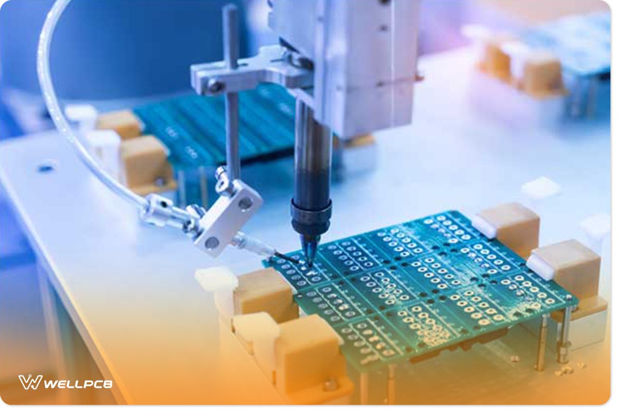
Glue Dispensing Machine
A glue dispensing machine applies precise glue dots to the surface of printed circuit boards (PCBs) before the components are placed. This machine is essential in PCB fabrication, as it holds components securely in position until their contacts and leads are soldered.
In wave soldering, the glue dispenser becomes particularly valuable. The high force of the solder wave can cause larger electronic components to shift or become displaced without the added stability the glue provides. During reflow soldering, the glue also prevents components from detaching as the board heats up, maintaining stability and alignment throughout the soldering process.

Pick-and-Place Machine
The pick-and-place machine is one of the most fascinating devices in PCB fabrication, especially when compared to other equipment. Watching it in action is impressive, as it carefully grasps components and places them onto the exposed PCB. This machine replaces the meticulous manual process of positioning components with tweezers, greatly improving efficiency and precision.
With this automated machine, PCB fabricators can operate around the clock, achieving a level of accuracy that surpasses human capabilities. Using suction, the pick-and-place device swiftly lifts surface mount technology components and places them precisely at their designated spots, previously marked by the glue dispensing machine. Operating at remarkable speeds, this machine can place up to 30,000 components per hour, making it an invaluable asset in efficient PCB production.

Reflow Soldering Machine
PCB fabrication mostly uses the reflow soldering method for accurate PCB assembly. The reflow soldering machine is a great and massive oven that deals with PCBs full of electronic components. You would see that the PCB boards move via different temperature zones that the machine would be carefully monitoring. Therefore, the solder paste dissolves and strengthens to develop robust electrical connections among the components and corresponding copper pads.

Wave Soldering Machine
The wave soldering machine for PCB fabrication passes the PCB through a molten solder wave for soldering the components. At the beginning of the wave soldering process, the machine will spread on the flux layer on the PCB surface. Will clean the components’ pads and contacts, and the solder will properly stick to the board.
After that, the machine warms up the PCB to avoid thermal shock. In the end, a molten solder container builds up a solder wave through which the PCBs pass in a way that their bottom comes in contact with the solder wave. The Develops a connection among the leads of the components and their corresponding pads and holes. Nonetheless, the reflow soldering machine has taken over wave soldering because of its effectiveness in soldering SMT components.

Automated Optical Inspection (AOI)
Finally, when the boards have undergone all PCB fabrication methods, you would send them for testing and inspection and testing. The automated optical inspection machine replaces the need for a hectic manual control. The naked eye cannot accurately inspect multiple PCB boards when they are produced on a large scale.
In PCB fabrication, AOI machines identify glitches in the PCB early on in the fabrication process. It utilizes HD cameras to take pictures of the board’s surface and then do its analysis. The machine compares the images with reference images to identify the faults. It will save wastage of PCB material and the cost of re-manufacturing. Moreover, this fixes the individual boards early, and the methods are accordingly modified.
In-Circuit Testing (ICT) – The Bed of Nails
The in-circuit testing phase uses a bed of nail fitting to inspect the working of complex PCB boards quickly. The testbed has an arrangement of pogo pins, and each one of them connects with nodes in the PCB circuit. The final PCB is put on these pogo pins and pushed downwards to make circuit board shopping, various things might get you confused. Whether you are going for a single-sided PCB, a double-sided PCB, or any other type of PCB, You can contact with test points. The pogo pins fitting quickly send test signals through the PCB via these test points. Therefore, it identifies any shorts or breaks in the circuit.

Functional Validation Test (FVT)
As the name implies, this test uses software to check if the PCB will work according to its function. It should be able to perform precisely what you want it to in your required field of application. The functional validation test interfaces the PCB through the test point or its connector for simulating the working environment.
The details of functional validation tests vary from product to product, as every PCB is unique. Commonly, the PCB fabricators personalize the hot mock-ups set up to simulate the final working environment. However, it does not matter how we customize the FVTs, as they all have the same software, hardware, and components.

X-ray
Many modern PCB designs include lead-less package types such as QFN and BGA assembly. These components make connections with PCBs under their bodies. Hence, traditional inspection methods are not efficient enough to inspect the internal structure of the PCB. The automated X-ray inspection method of PCB fabrication tests the hidden attributes of PCBs using X-rays.
To ensure the quality of the PCB fabrication process, an X-ray penetrates the PCB packages into the PCB package’s internal layers. It then examines the quality of soldering connections. The advantage of X-ray is that the PCB materials absorb it according to their thickness, atomic number, and density.
Conclusion
So, these were the 10 PCB fabrication and assembly techniques that you should know. Wne are hopeful that now you would see the big picture of what we are doing at the back-end. Wne fabricate high-quality PCBs using all of these machines and in no time. Feel free to development of flex PCB. Our dedication is to manufacture high-quality flex PCB. If you are looking for the right flex PCB manufacturer, contact us if you have any questions or want to ask for a quotation.


