Contents
1. PCB Mounting Hole Size

These holes are found on every PCB. They help in tying the PCB to the GND plane. The idea is that it is not possible to have the hardware soldered on a PCB.
In some cases, Vias is added to the supported mounting to help provide enough ground connections. It also helps to support the PCB when subjected to too much torque during the tightening of the nut.
Notice that other than using PCB mounting holes to secure your PCB enclosure, it is critical to note that they can be used to reduce Electromagnetic interference.
This is what is referred to as (EMI) reduction. It means PCBs considered sensitive to EMI should be placed in a metallic enclosure.
The plated PCB should be mounted on holes and connected to the ground. It helps to redirect electrical interference into the ground.
2. How to Design PCB Mounting Holes

Although simple, some rules should guide you when placing the holes.
Paying attention to the coordinates of the mounting holes is critical because if mistakes are made, it reduces the chances of having the PCB mounted as it should in its enclosure.
Correctly designed PCB holes allow for mounting of your PCBs in their enclosure.
3. PCB Hole Size Chart

A PCB hole chart provides general information on the holes and will guide you when placing components on your PCB.
Making the holes through which the components will be mounted is always challenging. Therefore, the tolerance and dimensions of the holes must be specified.
PCB charts play an important role here.
They specify the size of the holes that will ensure that your PCB is well-plated.
They also specify the software that will allow you to add holes to your PCB.
4. Standard PCB Hole Size

Traditionally, PCB holes were drilled using less advanced drills.
In most cases, the operators had to place the panels on X and Y coordinates before pulling the lever to drill holes.
The process was repeated many times until all the holes were drilled.
However, things have changed nowadays, and given that a PCB could have as many as 1000 holes drilled, using the traditional method will not guarantee you to drill enough holes in a PCB.
It has now become easier to drill holes using standard PCB drills. They utilize automated drilling machines designed for standard PCBs.
Drilling holes without following guidelines can result in holes that are too big or too small. First, you need to secure standard bits to use in drilling the holes.
Bits come in different sizes, and you may need to specify the hole size you need.
5. PCB Pad Hole Size Calculator

Calculating PCB hole size is not a difficult thing if you can follow the following steps:
First, you need to find the maximum diameter of the components, which will help you determine the shape and types of holes that you need to drill.
Notice that round holes are ideal if you will be using round PTH lead while the square shape is recommended when using square PTH lead.
For those who will be using rectangle PTH lead, rectangle holes may be suitable.
Generally, the minimum size will be calculated by looking at the maximum Lead Diameter +0.25mm, 0.20mm, or 0.15 mm, depending on the level of IPC.
The next thing you need to know is the size of the annular ring. It should be 0.05mm for level A, while for level B, it should be 0.5mm. For level C, it should be 0.4 mm.
It means that the Pad Diameter should be equivalent to the minimum home size plus minimum fabrication allowance plus minimum annular ring.
Note that levels A, B, and C represent the density levels. Level A is suitably used for low component density, while Level B is used for moderate Design reproducibility.
Normally, level B is preferred for reflow, drag, dip, or wave soldering.
On the other hand, Density level C is preferred when dealing with components with high density. It can be used in portable and handheld appliances.
6. How to Calculate PCB Hole Diameter

Normally, when calculating the PCB hole diameter, the aspect ratio between the hole’s diameter and the board’s thickness is considered.
If the thickness is 1.60mm, the hole size should be about 0.40. This means that the aspect ratio, in this case, is 1:4. Reducing the thickness of your PCB means that this ratio should also be reduced.
7. Hole Diameter: How to Calculate the Hole Size

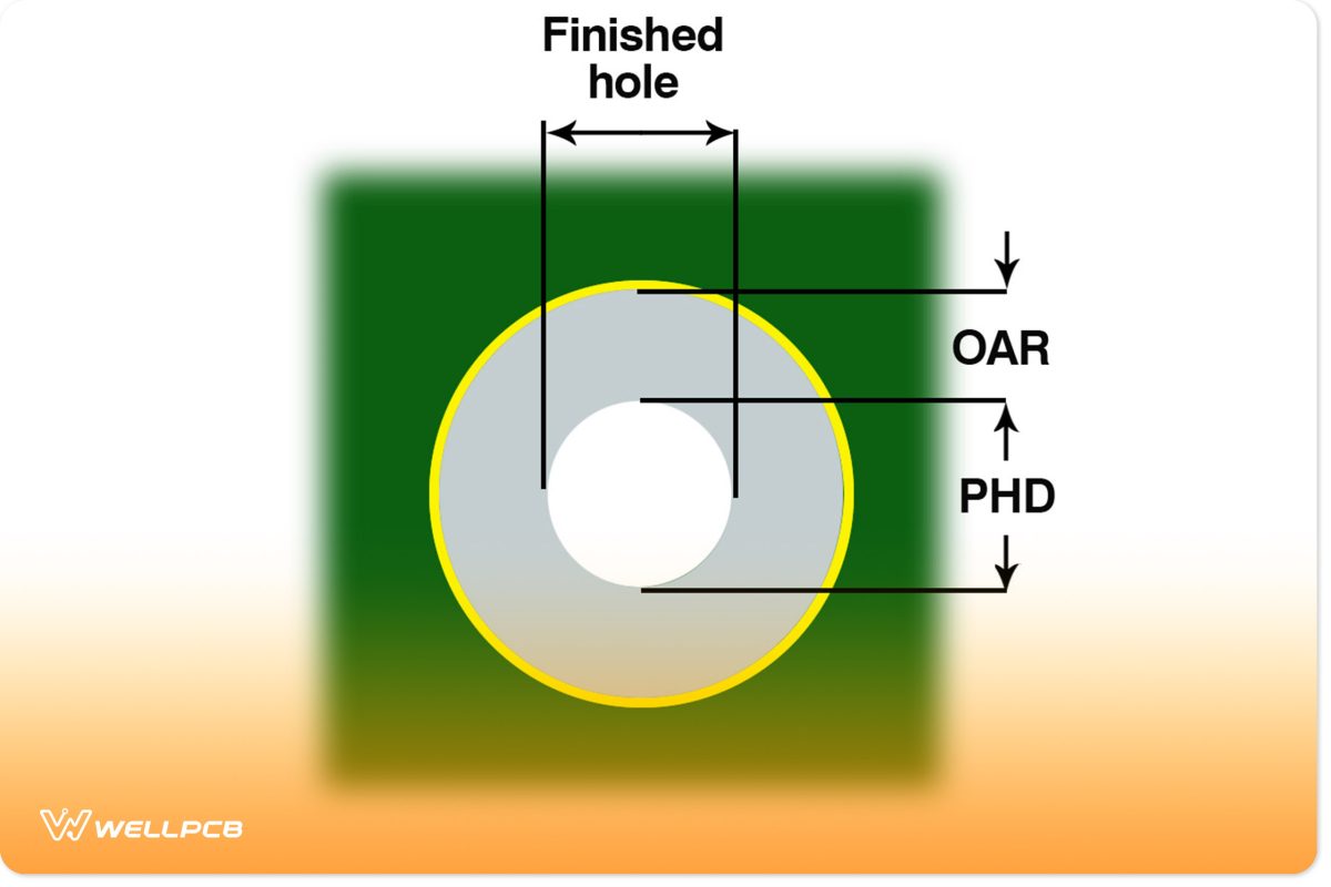
A hole diameter or PHD refers to a production tool’s diameter that you use to drill holes.
So, calculating a hole size diameter differed for non-plated through holes and plated through holes.
For a non-plated through-hole, the calculation is the sum of the finished hole size and +0.00mm/0mil.
But, plated through-hole, on the other hand, is the sum of the finished hole size and +0.10mm/4mil.

PCB hole diameter
Production Holes Diameter/PHD
The calculation for the PHD =
- Finished hole size + 0.00mm/0mil for Non-Plated Through Holes
- Finished hole size + 0.10mm/4mil for Plated Through Holes
- PHD – finished hole size = copper plating finish + applied finish
Hole Diameter–OAR (Outer layer Annular Ring)
The OAR is the outer layer annular ring. And you can calculate it by dividing the difference between the copper pad diameter and tool size by 2.

FAR (Finished Annular Ring)
The Finished Annular Ring is the part that lies between the solder hole and the external solder pad rim.
Plus, the annular ring breaks when the drilled hole is off the center.
But it all depends on the solder pad’s external diameter against the nominal hole size diameter.
Calculation of FAR;
The width (T1) of the finished annular ring on external layers should be >= 0.050 mm for the board.
The width (t2) of the annular ring on the inner layers should be >= 0.0100 mm for the board.


