
Contents
- 1 Demystifying Manufacturability: Why It Matters
- 2 Building a Manufacturable Design: Key Considerations
- 2.1 Material Selection: Choosing the Right Foundation
- 2.2 Electrical Performance and Trace Design
- 2.3 Drilling Considerations: Holes, Sizes, and Clearances
- 2.4 Component Placement and Routing Strategies
- 2.5 Integrating Test Points: Design for Testability
- 2.6 Clear and Complete Design Documentation: The Missing Piece
- 3 The Power of Collaboration: Working With a Reliable PCB Manufacturer
- 4 Ready To Discuss Your Next Project? Contact Our Engineering Team!
Demystifying Manufacturability: Why It Matters
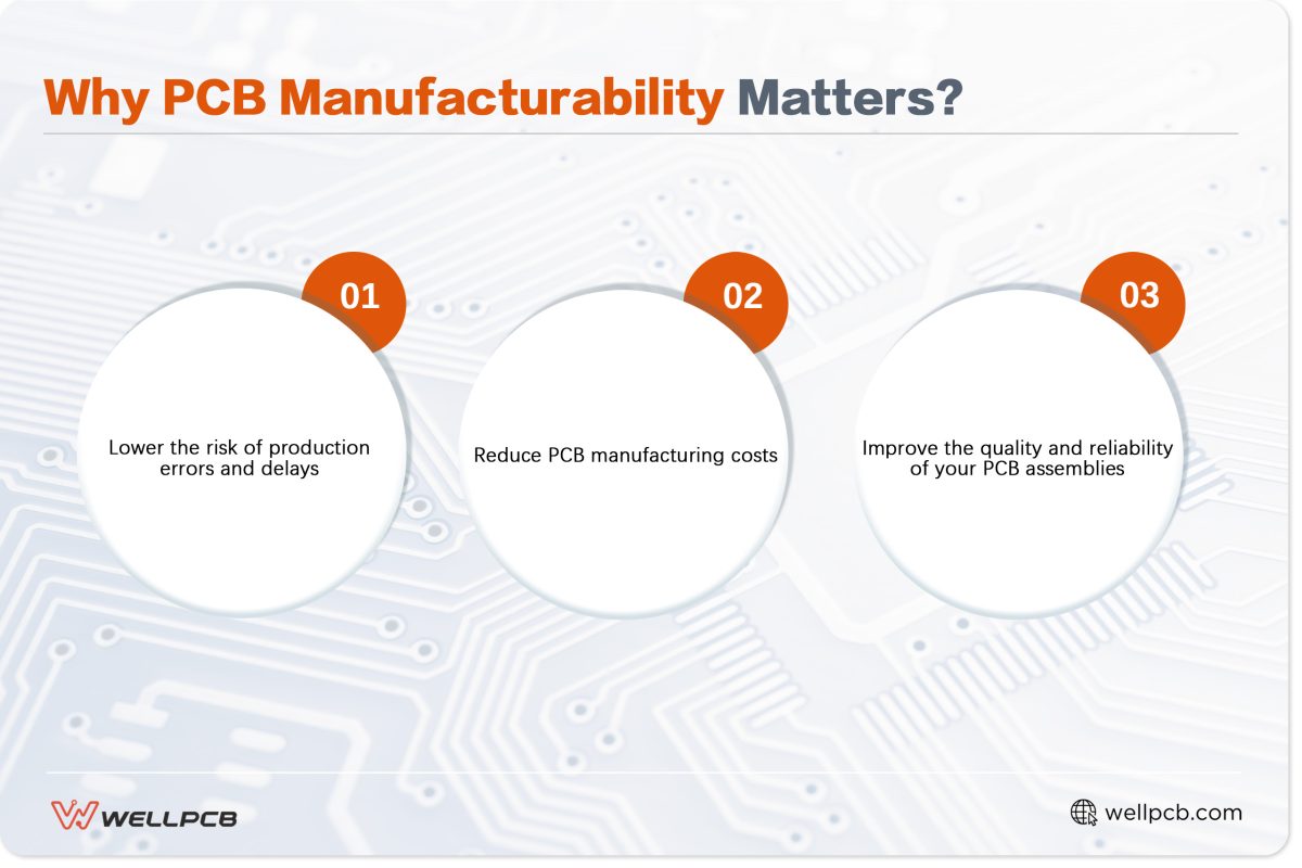
Why does PCB manufacturability matter?
‘PCB manufacturability’ refers to how effectively manufacturers can fabricate and assemble your PCB design. By designing for manufacturability (DFM), you can:
- Lower the risk of production errors and delays: Designs that adhere to manufacturability guidelines align with the capabilities of the PCB fabricator.
- By following these guidelines, you can reduce the likelihood of issues such as trace shorts, opens, and misalignments—common problems that can lead to production delays and increased costs due to rework and scrap.
- Incorporating these practices into circuit board manufacturing helps streamline production, ensuring efficiency and cost-effectiveness from the start.
- Reduce PCB manufacturing costs: There are several upsides to avoiding overly complex designs, selecting standard materials, and ensuring efficient panelization during PCB fabrication. You can minimize material waste, reduce processing times, and use cost-effective PCB production techniques.
- Improve the quality and reliability of your PCB assemblies: This includes proper trace routing, appropriate component placement, and adherence to design rules, all of which ensure that the final product meets performance specifications and operates reliably over its intended lifespan.
Building a Manufacturable Design: Key Considerations
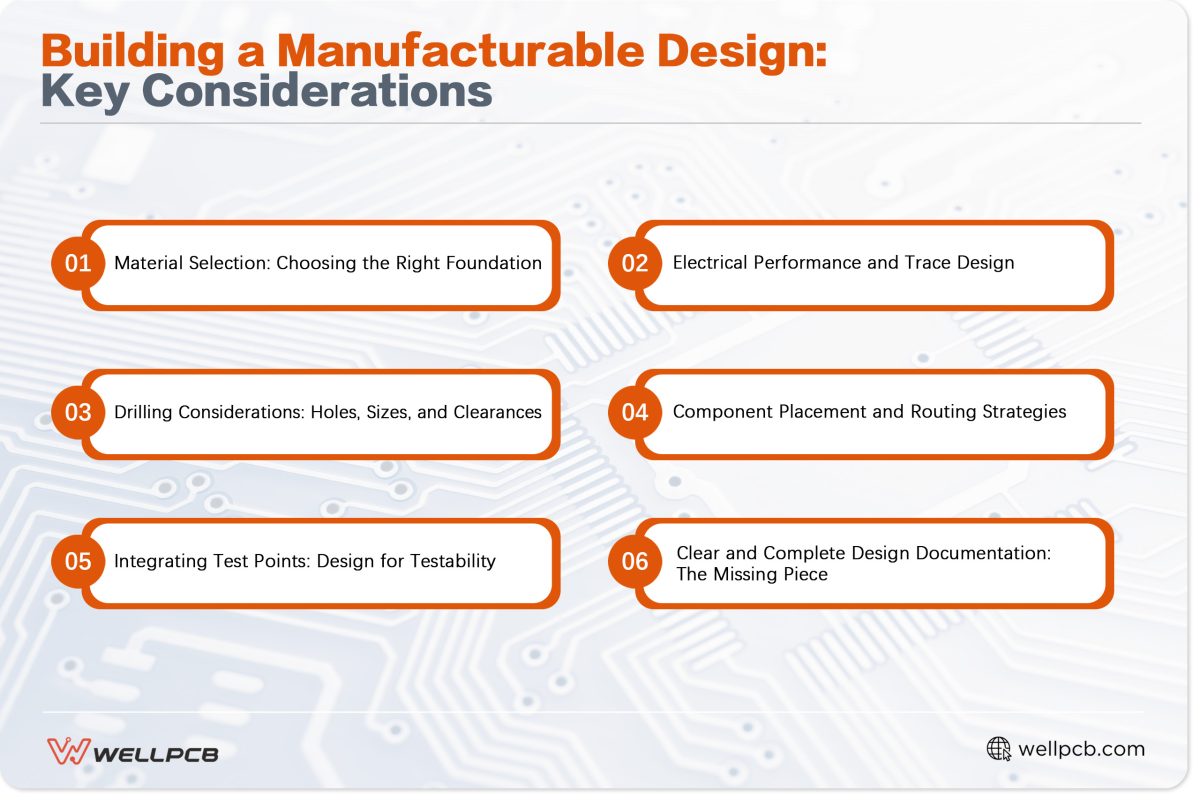
Implementing a few crucial DFM principles in your PCB design process ensures efficient manufacturability of your circuit boards. Ultimately, these principles are guidelines for planning and structuring your PCB layout for the manufacturers.
Material Selection: Choosing the Right Foundation
As more electronics companies grow conscious of their impact on the environment, designers must be considerate of the materials they choose for their circuit boards.
These decisions will affect not only the cost and sustainability of the PCB manufacturing process but also the recyclability of the PCBs.
We recommend that you consult the following IPC guidelines where they apply to the type of circuit board you’re designing:
- IPC-2221: A general standard for all printed circuit board designs
- IPC-2222: A sectional design standard for rigid organic printed boards
- IPC-2223: A sectional design standard for flexible and rigid-flex boards
- IPC-2226: A sectional design standard for high-density interconnect (HDI) printed circuit boards
- IPC-2228: A sectional design standard for high-frequency (RF/Microwave) printed boards
Generally, the material you choose for each key part of your PCB should satisfy a few requirements. These requirements include operating and soldering temperatures, interconnections, structural strength and stability, circuit density, and flame resistance.
Once you determine these parameters, you can use them to select the dielectric material for the PCB’s substrate. The most common are as follows:
- FR-4 (Epoxy E-glass)
- Multi-functional Epoxy
- High-Performance Epoxy
- Bismaleimide Triazine/Epoxy
- Polyimide
- Cyanite
The PCB layout will determine the types of materials you’ll need and influence the required amount or volume of said materials.
For instance, the electrical property and overall thickness tolerance requirements will impact your PCB assembly’s copper layer thickness and weight.
These factors, in turn, impact the board’s thermal stability, which you will need to offset by introducing additional materials, such as thermally insulating adhesives.
It’s important to remember that the materials you select should balance all of these requirements and parameters.
Electrical Performance and Trace Design
Trace location and size have significant ramifications on your PCB’s electrical performance.
According to IPC-2221, the trace width for standard PCBs should range between 7 mils (0.177 mm) and 12 mils (0.30 mm).
Minimum trace spacing should be 10 mil (0.25 mm) for low-voltage applications and 20 mil (0.5 mm) for high-voltage boards and components.
Another factor to consider is the application of conformal coating. This can also impact the electrical performance of your boards.
For instance, many surface-mount technology components tend to perform poorly without conformal coating. This is primarily because of tight lead and land trace spacing.
Regardless, you must ensure that any additional conformal coating application doesn’t impede your PCB’s electrical performance.
This means your PCB needs sufficient masking and protection.
The more advanced the structure of your printed circuit board is, the more consideration you’ll have to give to power and ground trace distribution.
For instance, we highly recommend using (power and ground) planes to optimize signal integrity for multilayer PCBs.
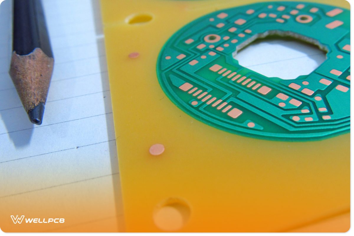
Drilling Considerations: Holes, Sizes, and Clearances
Drilling can often be the most expensive and complex phase in the PCB assembly process.
The smallest mistake in positioning or measurement can ruin an entire batch of printed circuit boards and lead to considerable losses.
However, drilling is extremely important, as it is the first step to establishing vias and interconnectivity between the PCB’s inner and outer layers.
There are two main types of drilling technologies: laser and mechanical.
Laser drills are more precise and can easily produce holes with a diameter of 2 mils (0.050 mm). In contrast, the smallest hole a mechanical drill can produce is a 6 mil (0.152 mm) diameter.

Drilling Technologies
Nevertheless, mechanical drills are less costly than their laser-based counterparts.
Regardless of your technology, you must ensure your drill holes meet the IPC’s basic guidelines on aspect ratio and drill-to-copper clearance. The aspect ratio will influence how easily the manufacturer can plate copper foil into the holes to produce vias. It will also ultimately impact the hole tolerance for the design’s manufacturability.
You can calculate the aspect ratio by dividing the hole depth by diameter (AR = Depth/Diameter). Generally, the aspect ratio for micro-vias is 0.75:1 and 10:1 for through holes.
The drill-to-copper clearance refers to the section between the nearest copper feature (trace or pads) and the edge of the drilled hole.
Insufficient drill-to-copper clearance can result in circuit disruptions.
The general rule of thumb is a minimum drill-to-copper value of 8 mils (0.203 mm).
However, you can gather a more precise minimum value by adding the annular ring width to the solder mask dam clearance.
Component Placement and Routing Strategies
Optimizing the placement of the components can maximize the speed of the PCB manufacturing process.
The first step is to identify the location of the PCB’s input and output connectors and then plan your component placement.
This will ensure your components integrate well with the signal flow while minimizing the routing complexity.
It’s always a good idea to produce a rough floor plan and schematics to determine the best location for each component.
Rough sketching for PCB floor plan
You should use the following order to arrange components:
- Connectors and circuit protection components (along the edge of the circuit board)
- Integrated circuits
- Active auxiliary components such as decoupling capacitors
- Passive components
Similar components should be oriented the same way. This makes them easier to place and solder. Put all through-hole components on the top side of the board.
It’s also best to position all surface mount technology (SMT) components on the same side of the board.
Spacing is the most critical aspect of component placement during PCB fabrication.
In this case, it is best to consult and follow IPC-1222’s spacing guidelines for PCB components.
It’s also important to separate lead components from lead-free components and implement independent, well-proportioned pads for all component connections.
When placing components, be aware of the weight distribution across the board. Aim to keep it as consistent as possible.
Integrating Test Points: Design for Testability
Onboard faults and errors can occur despite how extensively you prepare and plan. So, it’s important to incorporate test points to ease troubleshooting and refurbishment.
Test points are essentially access areas for test probes. They allow you to test signals through a PCB and monitor the functionality of its circuitry.
Follow these best practices for test point placement:
- Place the test points on a single side of the board
- Test points should be distributed evenly with the distance between them not exceeding 100 mils (2.54 mm)
- Organize components in such a way that allows for efficient test point placement
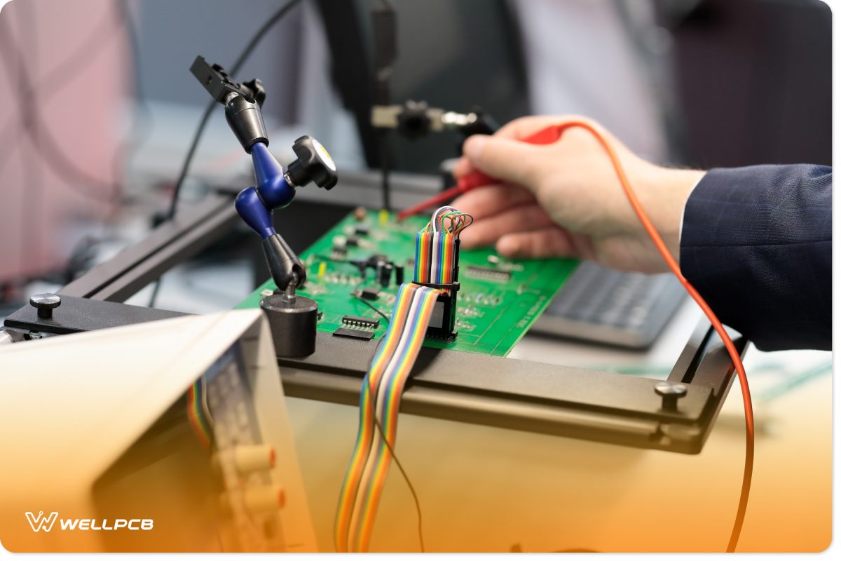
PCB testing and quality control with oscilloscope
Clear and Complete Design Documentation: The Missing Piece
All PCB designs should be accompanied by clear, comprehensive documentation. This includes:
- Schematics (Gerber files)
- Bill of materials (BOM)
- Manufacturing data (centroid file)
These documents will minimize errors during the PCB manufacturing process and ensure your PCBs are fabricated as seamlessly as possible.
The Power of Collaboration: Working With a Reliable PCB Manufacturer
When scouting for a PCB manufacturer, take some time to read reviews and testimonials from past clients before making a decision.
It’s best to partner with a manufacturer that focuses on DFM. This will ensure the reliability of the production process while ensuring the quality of your boards.
Select a manufacturer that offers DFM review services. A competent PCB manufacturer should be able to assess and even improve your design’s manufacturability.
The PCB manufacturer should also have multiple lines of communication and be available to address your queries promptly.
They should be familiar with modern DFM industry standards and committed to strict quality control during printed circuit board manufacturing.
Ready To Discuss Your Next Project? Contact Our Engineering Team!
You may have noticed that many concepts in PCB manufacturing are related. For instance, test point positioning cannot be addressed without considering electronic component placement.
These are the nuances you should consider when planning your next design.
Consulting with one of our engineers can ease and accelerate the entire process. Contact us today and learn how we optimize the manufacturability of your PCB design.


