
Contents
- 1 Do You Understand the Basics of PCB Manufacturing?
- 2 What Steps Are Involved in The PCB Manufacturing Process?
- 2.1 Step 1: Design and Layout
- 2.2 Step 2: Printing the PCB Design
- 2.3 Step 3: Copper Printing and Etching
- 2.4 Step 4: Layer Alignment and Lamination
- 2.5 Step 5: Drilling
- 2.6 Step 6: Plating
- 2.7 Step 7: Solder Mask Application
- 2.8 Step 8: Silkscreen Printing
- 2.9 Step 9: Surface Finish
- 2.10 Step 10: Electrical Testing
- 2.11 Step 11: Final Inspection and Quality Control
- 3 What Unique Techniques and Innovations Exist in PCB Manufacturing?
- 4 Proprietary Techniques Our Company Uses
- 5 What are Some Common PCB Production Challenges and How Do You Overcome Them?
- 6 Choose WellPCB for Your PCB Needs
Do You Understand the Basics of PCB Manufacturing?
What Is a PCB?
Printed circuit boards (PCBs) are flat slabs of insulating laminate and conductive material. The main purpose of a PCB is to power and connect various components in an electronic device.
For example, your smartphone has a speaker, sensors, screen, various ports, and a rechargeable battery. Connecting and powering these components is a PCB, which distributes power from the battery and enables communication between them.
There are three main types of PCBs:
- Single-sided PCB: A single-layer circuit board that accommodates electronic components on one side.
- Double-sided PCB: A double-layered circuit board that accommodates electronics on both sides.
- Multilayer PCB: This circuit board consists of three or more layers, allowing for more complex and dense circuit designs.
Key Components of a PCB
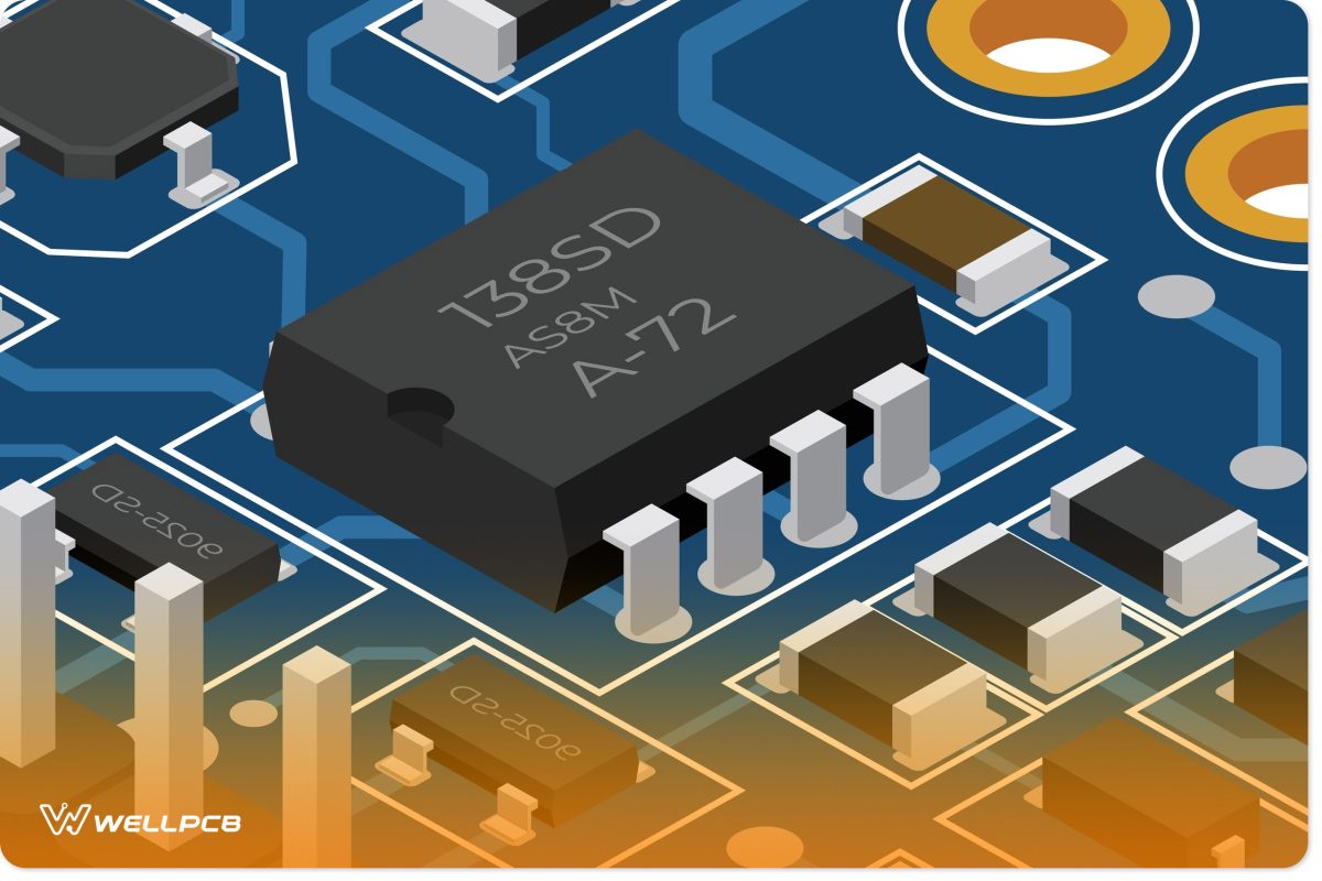
Every PCB has several key parts:
- Substrate/laminate: This non-conductive base layer, which is usually made of fiberglass, provides structural support.
- Conductive layer(s): These layers, typically made of copper, allow electric currents and signals to pass through the PCB.
- Solder mask: This component is applied to conductive traces, protecting them from oxidation and preventing solder bridging.
- Silkscreen: This is used to mark component locations and provide information about the PCB.
What Steps Are Involved in The PCB Manufacturing Process?

Step 1: Design and Layout
The PCB design phase comprises two parts: schematic capture and PCB layout planning.
Schematic capture involves blueprinting and diagramming the circuitry, while PCB layout planning involves designing the physical board.
2D and/or 3D models of the PCB are often created in this process.
Modern PCB designers use various Computer Aided Design (CAD) software tools, such as Eagle PCB, Altium Designer, Autodesk, and ExpressPCB.
The feature sets of these tools allow designers to work on both PCB design and layout.
When designing your PCB, pay attention to the circuit, component placement, and routing.
After routing, ensure your PCB has clear electrical return paths that can add power and ground planes.
Before finalizing and printing the PCB, a Design Rule Check (DRC) is required.
This will verify the manufacturability of your PCB layout by searching for errors in the preset width trace, clearance, hole size, and annular ring dimensions.
Step 2: Printing the PCB Design
Once the DRC is complete, the PCB manufacturer uses a plotter to create a film sheet of the design.
The plotter can use either photolithography or direct imaging to produce the sheet. Both methods yield highly precise x-ray-like photo-negative images of the PCB.
The black portions of the image represent the copper traces and circuits of the PCB, while the clear portions indicate the non-conductive areas.
Accuracy and precision are vital during this step, as any mistake can render the entire batch of PCBs useless.
Each layer and solder mask of the PCB receives a unique sheet of film.
Once printed, the manufacturer aligns the sheets and punches a registration hole through them to ensure all layers align correctly during fabrication.
Step 3: Copper Printing and Etching
The manufacturer prints the PCB design onto a laminate slab, then pre-bonds a sheet of copper to it.
Excess copper is then removed from the board through etching, exposing the layout design printed in the previous step.
Next, photolithography is used to mark and protect the intended copper pathways. The board is then washed with an alkaline solution to remove excess photoresist material remaining from the photolithography process.
The manufacturer then pressure-washes the board to ensure it’s free of impurities. Once dry, an inspector verifies that the board has no defects.
Step 4: Layer Alignment and Lamination
Multilayer boards require additional preparation, printing, and etching — as each of the previous steps needs to be completed for each layer.
Once these steps are done, all the layers of the PCB are aligned, and a post-etch hole is punched through them using a computer-guided machine known as an optical punch.
The manufacturer then performs an Automated Optical Inspection (AOI) test on the punched layers of the PCB.
Once verification is complete, the oxide is applied between the layers to enhance bonding. A machine then stacks the layers and applies heat and pressure.
This melts the bonding agents (typically epoxy resin) between the layers, essentially laminating the PCB.
Step 5: Drilling
X-ray imaging is used with the design layout to identify areas of the PCB panel that require drilling. Once identified, the manufacturer drills mounting holes and vias.
Most drilling is computer-guided for precision.
Mechanical drills are used for larger holes (mounting holes), while lasers are used for smaller, more precise holes.
Once drilling is complete, the PCB is cleaned and prepared for plating.
Step 6: Plating
The manufacturer then dips the panel in a combination of chemicals to plate the drilled holes, applying a micrometer-thin layer of copper to the PCB panel.
The copper enters the drilled holes, covering their exposed fiberglass walls.
This allows through holes and blind vias to connect to the conductive pathways and layers of the board.
Once plating is complete, the panel undergoes another imaging process where a sheet of photoresist is applied.
Using imaging as a guide, the manufacturer then applies a protective layer of tin to the panel’s conductive sections and etches copper away from the non-conductive parts.
The manufacturer then removes any excess photoresist and returns the PCB panel for another AOI and solder mask application.
Step 7: Solder Mask Application
The solder mask is a thin layer of polymer that protects the exposed conductive elements from oxidation and helps prevent solder bridges, making it an essential component of the PCB manufacturing process.
Before applying the solder mask, the manufacturer thoroughly cleans the panel and applies an ink epoxy.
The epoxy reveals the parts of the board that should remain free from the solder mask coating.
The manufacturer then applies the solder mask and exposes the board to ultraviolet light, which hardens the ink epoxy.
Using the epoxy as a guide, the manufacturer removes the solder mask from the marked areas.
Finally, the board is placed in an oven to harden and cure the remaining solder mask.
Step 8: Silkscreen Printing
Silk printing allows the manufacturer to mark and label the PCB with important information, such as:
- Part/serial number
- Manufacturer information
- Company identification number
- Warning labels
- Via and component markings
- Test point markings
The silk-screen printing process usually applies white epoxy ink to the component side of the PCB.
Other colors can be used, such as yellow, red, and black, though this will depend on factors such as client requirements and solder mask color.
Step 9: Surface Finish
The final step in the fabrication process involves applying a protective layer to the PCB, referred to as the surface finish.
This layer protects the conductive elements from oxidation and erosion.
A wide range of surface finishes are available, with immersion gold (ENIG) often considered the best due to its lead-free composition and long shelf life. Other options include:
- Immersion silver
- Immersion tin
- Hard gold
- Electroless nickel immersion gold (ENIG)
- Hot air solder leveling (HASL), both leaded and unleaded
- Organic solderability preservative (OSP)
- Electroless nickel electroless palladium immersion gold (ENEPIG)
The choice of surface finish will depend on the client’s budget and specifications.
We recommend selecting a finish that’s environmentally friendly and effective in preventing oxidation.
Step 10: Electrical Testing
A technician performs a collection of electrical tests to ensure there are no shorts or defects. There are two main types of assessments: circuitry continuity and isolation testing.
- Circuitry continuity checks for any “opens” in the circuitry, which are essentially disconnections or interruptions.
- Isolation testing isolates each PCB component to check for any shorts.
The PCB manufacturer may also use more intrusive methods of testing, such as in-circuit or “bed of nails” tests.
Step 11: Final Inspection and Quality Control
The manufacturer then profiles and cuts each PCB from its panel.
A technician performs a final inspection of the boards to verify that all hole sizes are consistent and that the board dimensions match those in the specifications.
They also ensure that each board is free from rough or sharp edges, dust, and other impurities. Boards that fail inspection must be repaired and re-tested.
Once testing and quality control are complete, the manufacturer can package and ship the boards.
What Unique Techniques and Innovations Exist in PCB Manufacturing?
Proprietary Techniques Our Company Uses
WellPCB offers full DRC as part of our service offering, guiding you from the design phase to the final production and packaging.
Our one-stop fabrication and assembly services are guaranteed to meet all your requirements.
We handle the entire process, from fabricating the PCB and procuring necessary components to assembling the final product.
WellPCB supports full Ball Grid Array (BGA) and Micro-BGA installations.
We use the latest technology in electrical testing and inspection, including AOI and X-ray inspection.
We also offer full refunds or free reworks for any board faults we may have missed.
Industry Innovations and Trends
Environmental sustainability is an enduring industry trend that continues to drive significant innovation.
Manufacturers and companies aren’t moving away from environmentally unsustainable practices entirely out of virtue; they’re increasingly mandated by government legislation.
The materials used in PCB manufacturing offer a clear opportunity to adopt more sustainable practices.
In fact, designers and manufacturers on the cutting edge are already developing recyclable and biodegradable PCBs to combat e-waste.
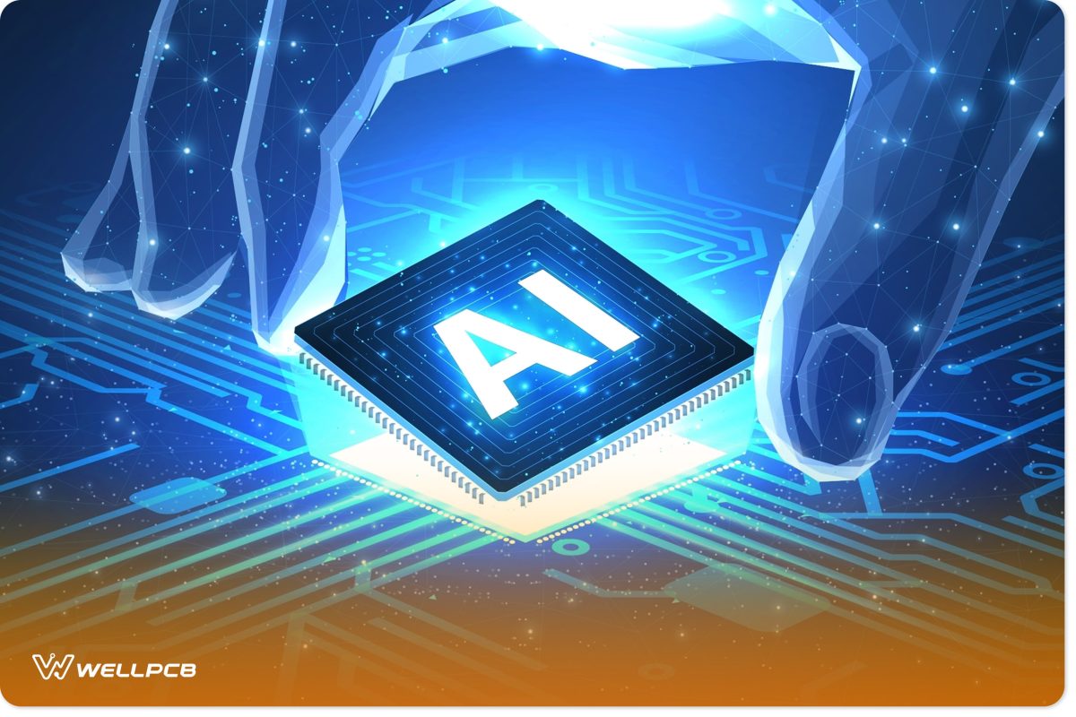
Artificial intelligence has revolutionized the PCB and semiconductor industries.
Much of this technology runs on graphical process units (GPUs) that use HDI PCBs, which can be highly complex, time-consuming, and expensive to produce.
As such, the industry is likely to continue developing more efficient and cost-effective production methods.
What are Some Common PCB Production Challenges and How Do You Overcome Them?
Design Challenges
Some common PCB design challenges include:
- Starved thermals
- Acid traps
- Silvers
- Insufficient annular ring
- Via in pads
- Copper to the board edge
- Missing solder mask between pads
- Tombstombing
These issues can be addressed by performing the necessary design rule checks before fabrication. This allows the fabricator to verify that the design meets the required tolerances.
Manufacturing Challenges
The two most common manufacturing challenges are supply chain shortages and outdated or broken machinery.
- Supply chain shortages: These can be difficult to manage, but manufacturers should strive to keep non-perishable stock on hand and source from diverse suppliers.
- Outdated and broken machinery: Manufacturers must maintain and replace equipment regularly, aiming to have the latest state-of-the-art machinery. This ensures maximum efficiency and supports the latest manufacturing requirements and trends.
Before deciding on a manufacturer, potential clients and customers should thoroughly research all candidates.
Online client or customer reviews can offer valuable insights. Selecting a reputable and experienced PCB manufacturer is vital, as this lowers the risk of design and manufacturing issues.
Quality Control Challenges
Thoroughly testing a large production run can be complicated, so most manufacturers use large automated systems as opposed to individual inspectors and technicians.
However, these systems are not perfect, and certain aspects of quality control and inspection cannot yet be reliably automated.
To address this, PCB manufacturers must employ skilled laborers and quality control experts who can ensure that all PCBs and assemblies are fault-free.
When assessing PCB quality, standards such as the IPC-9252 should be followed strictly.
These guidelines provide testing and quality control standards that all PCB manufacturers should follow.
By adhering to these rules, manufacturers can overcome most, if not all, quality control challenges.
Choose WellPCB for Your PCB Needs
The PCB manufacturing process is complex with multiple stages. From design to drilling to silkscreening, every step is vital to ensure a high-quality and fault-free product.
However, not all manufacturers are equal. Simply offering or performing all necessary steps does not guarantee a flawless PCB.
As such, it’s essential to partner with a reputable and experienced PCB manufacturer to ensure high-quality results, like WellPCB.
We support PCB fabrication and assemblies of all sizes, with no minimum quantity requirements and with prices that are flexible and accommodating.
We adhere to the latest RoHS standards and package our orders in safe, anti-static, shockproof boxes.
Generate an online quote today and discover how we can save you time and money on your next project.


