
Contents
- 1 How Does PCB Trace Technology Work?
- 2 Why Is PCB Trace Design Useful?
- 3 What Is the Manufacturing Process of PCB Traces?
- 4 What Makes a PCB Trace High-Quality?
- 5 What Considerations Should You Have for Your High-Quality PCB Trace Design?
- 6 Modern PCB Trace Design Techniques for Best Results
- 7 Use Expert PCB Assembly Services
How Does PCB Trace Technology Work?
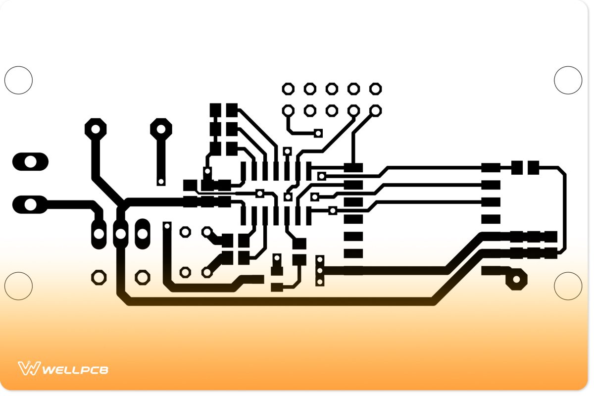
Traces distribute electronic and digital signals throughout the PCB, powering and enabling various components to function effectively.
These traces are typically thin paths of conductive material, usually copper. While they play a vital role in the PCB’s power delivery network (PDN), traces are just one part of PCB trace design.
Other important elements include pads and vias. Pads are specific areas on the PCB where component connections are made, while vias connect the various conductive layers of the PCB, enabling the routing and switching of trace connections.
For more insights on how these components work together in PCBs, check out our PCB Assembly Guide – PCB 101. For designs requiring both flexibility and durability, and rigid-flex PCBs offer an ideal solution, combining multiple functionalities in one board.
[Image: Traces On Printed Circuit Board]
Why Is PCB Trace Design Useful?
Designers and engineers can’t afford to take for granted the importance of proper routing and trace laying. Implementing optimal PCB trace design can enhance the overall performance and quality of your printed circuit boards.
As the introduction mentions, traces make up the circuitry connecting all your PCB’s components. Many of these components alter the intensity and nature of electric current. For instance, circuits use resistors to decrease the flow of the current.
Using improper trace design can lead to unintended outcomes. For instance, you may apply too little (or too much) resistance to the current, which can lead to dysfunctional or damaged boards.
Since high-speed digital PCB designs are far more complex than their analog counterparts, optimal PCB trace design is even more crucial.
These systems have more intricate power delivery demands. In addition to this, you need to position and structure traces in such a way that they deliver and maintain signal integrity.
In the real world, carefully designed traces can result in benefits such as:
- Optimized power delivery in complex systems: Efficient power distribution across components helps to prevent voltage drops and power losses in advanced electronics.
- Enhanced signal integrity in high-speed circuits: Reduced crosstalk and noise in circuits operating at high frequencies improves overall performance.
- Enabling IoT and wearable devices: Compact and optimized trace layouts are essential for reducing power consumption and size in IoT devices and wearables, prolonging their battery life and improving functionality.
- Minimizing electromagnetic interference (EMI): With reduced EMI, sensitive components can better function without external noise.
What Is the Manufacturing Process of PCB Traces?
As manufacturers, we dedicate a substantial portion of the PCB fabrication process to traces.
After all, the traces have to be able to facilitate accurate and strong connections between the components of the printed circuit board.
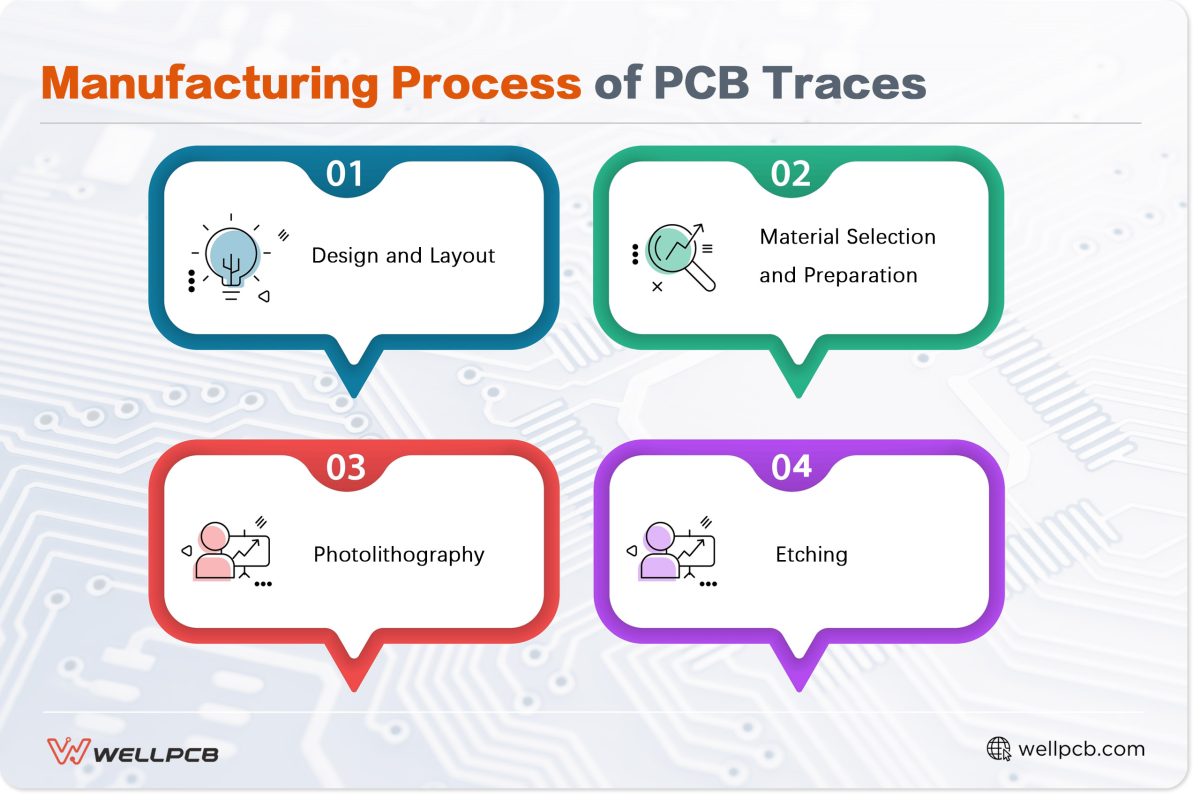
From start to finish, here are the steps we follow during the trace manufacturing process:
Design and Layout
First, a designer plans and outlays the trace and component placement of the PCB. The designer typically accomplishes this using computer-aided design (CAD) software. This makes the design process more efficient and accurate.
Material Selection and Preparation
The designer and manufacturer select and source the materials required for manufacturing. Traces would be useless without a base to hold, insulate, and protect them.
First, we apply adhesive resin to a slab of laminate material. This material typically consists of fiberglass. Once the resin dries, we place a copper foil on each side of the slab.
After some application of heat and pressure, the copper bonds to the slabs, resulting in what is known as a copper-clad laminate (CCL).
It’s also crucial to consider applying conformal coating at this stage to protect the traces from environmental factors.
Photolithography
At this point, there is no real delineation between the traces and the substrate material, and we can’t form the traces without guidance. As such, we need to use photolithography to lay down an outline for the traces.
The process starts with printing the PCB trace outline on a photoresist sheet and applying it to the CCL’s surface.
Then, we use a blast of UV light to transfer the trace outline from the photoresist to the CCL.
After that, we remove the portions of the photoresist that don’t contain an outline from the CCL.
Etching
The next step allows us to physically form and shape the traces. We use a chemical to etch away any copper not covered with photoresist.
This exposes the laminate slab underneath and leaves the copper traces behind.
After etching, the next steps include drilling and plating vias and through holes. From there, we add the finishing touches to the PCB, such as a solder mask, silkscreen labels, and surface finish.
Before the PCB is ready for packing and shipment, it must undergo electrical testing. This is to ascertain the quality of the traces and ensure there aren’t any flaws, such as open and short circuits.
What Makes a PCB Trace High-Quality?
A lack of flaws or interruptions in the trace’s structure is one factor in determining the quality of the PCB trace. However, it doesn’t tell us the entire story.
First, we need to consider the material type. As we mentioned previously, copper is the most widespread trace material.
This is mainly because it offers low resistivity and high conductance. The performance and reliability of copper traces depend on their thickness and weight.
The rule of thumb is the thicker the copper, the more current carrying capacity it has.
Most guidelines represent copper weight in ounces per foot square (oz/ft^2), which equates to 1.37 mils (35 μm) in weight.
Copper traces have three different weight/thickness ranges:
- Standard: 0.5 oz/ft^2 (17.5 μm) to 1 oz/ft^2 (35 μm)
- High/Heavy: 2 oz/ft^2 (69.59 μm) to 20 oz/ft^2 (711 μm)
- Extreme: 24 oz/ft^2 (853.44 μm) to 200 oz/ft^2 (7112 μm)
1 oz/ft^2 is the standard copper weight for printed circuit boards. The thickness and weight of your traces (copper or not) will impact all trace-related design requirements for your board.
This includes the minimum annular ring size, PCB trace width and spacing, and minimum conductor clearance (external and internal layers).
The amount of copper you use will also affect the weight and total cost of the PCB.
Trace weight and thickness may play the most important role in your PCB’s electrical performance. However, other factors can diminish or help improve it—namely the surface finish.
How Surface Finishes Impact Traces
Copper is highly susceptible to oxidation and corrosion. This can tarnish it over time and diminish its performance, even in unpolluted environments. Adding a protectant to it helps to prolong its lifespan, which is the purpose of a surface finish.
In addition to protection, surface finishes increase the solderability of PCBs by easing the formation of solder joints.
Some surface finishes can improve the performance of the trace by eliminating the skin effect. This is where the electrical current runs on the conductor’s surface instead of evenly distributed across its body. The skin effect can lead to poor thermal management and performance dips, particularly in high-frequency PCBs.
Electroless Nickel Immersion Gold (ENIG) and Immersion Silver (ImAg) both offer excellent solderability and electrical performance.
The use of ENIG, in particular, provides a flat, smooth finish, which can reduce the occurrence of the skin effect.
Both these surface finishes pair well with copper. However, remember that copper isn’t the only conductive material you can use for traces.
In fact, instead of using a gold or silver-based solder finish, you can also use these materials for your PCB’s conductive layer.
Alternative PCB Trace Material
The most noteworthy alternative materials for PCB traces are:
- Gold: Substantially more expensive than copper and less available. However, because of its resistance to corrosion and its high conductivity, gold is ideal for high-reliability use cases. For example, ceramic radio frequency (RF) printed circuit boards for aerospace equipment.
- Aluminum: A lighter and less expensive solution to copper. However, it doesn’t offer as much conductivity and is as susceptible to oxidation as copper. So, we mostly employ it in PCBs where weight may be a factor but not necessarily electrical performance.
- Silver: Like gold, it’s more expensive than copper but delivers superior performance. As such, manufacturers build silver-based PCBs for high-performance use cases.
While these are the most common materials, they’re not the only ones available for constructing traces.
New and Emerging PCB Trace Materials
Here are some lesser-known emerging materials that could potentially have a huge impact on printed circuit board production in the future:
- Graphene: Displays exceptional electrical conductivity, heat dissipation, and mechanical strength. Additionally, it’s thin and lightweight, making it ideal for flex and rigid-flex PCBs.
For now, the industry has mainly sought to use graphene to enhance the properties of copper traces rather than replace them entirely. Coating copper traces in graphene allows us to reap the benefits of both materials.
- Advanced alloys: Advanced alloys (also known as superalloys or high-performance alloys) are a mixture of metals or conductive materials, for example, silver and copper. They perform exceptionally well in aerospace, industrial, and high-performance electronics because of their superior electrical conductivity, heat resistance, and mechanical strength.
- Polymers: PCBs mostly use polymers in their dielectric material. However, not all polymers or polymer-based materials are non-conductive. Polyaniline and PEDOT are examples of conductive materials we can use to build traces.
The greatest advantage of these materials is that we can adjust their electrical properties through chemical doping.
They’re also flexible and lightweight, making them suitable for flexible circuits in medical devices and wearable consumer products.
What Considerations Should You Have for Your High-Quality PCB Trace Design?
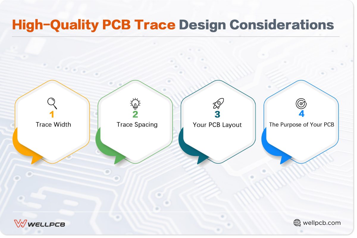
As previously discussed, the material you use and its thickness will impact the other parameters of your PCB. Let’s take a look at some of these parameters in more depth.
Trace Width
The width of the PCB’s traces will affect values such as current carrying capacity, signal integrity, thermal management, and voltage performance.
Here, the wider the traces, the better their ability to perform the task at hand.
At any rate, your PCB trace width must conform to your board’s space constraints and manufacturability. Wider traces limit the space for other electronic components. They can also restrict trace spacing.
Trace Spacing
If you place the traces too closely to one another, it can cause signal integrity issues.
Traces (like most conductors) generate electromagnetic fields.
The fields of adjacent traces can negatively affect each other, resulting in electromagnetic interference.
You can limit crosstalk, ensure voltage isolation, and encourage heat dissipation by employing optimal trace spacing. It’s always best to consult the necessary regulations and standards for trace width and spacing.
Your PCB Layout
The primary purpose of traces is to form electronic circuits that connect the various components of the board.
Therefore, the proposed PCB layout and the specific requirements of your components will shape the design of your traces.
When creating your PCB design, you’ll need to consider the position of your pads, through holes, and vias relative to the location of your traces. Doing so will help to ensure proper connectivity and performance.
The Purpose of Your PCB
Your printed circuit board’s general component and package density hinges on its ultimate purpose. For instance, high-intensity PCBs like motherboards have higher performance and conductivity demands.
As a result, they have different requirements for PCB trace thickness, trace material, surface finish, and spacing.
Modern PCB Trace Design Techniques for Best Results
As advanced as modern PCB design and manufacturing have become, the fundamental role of traces remains unchanged.
However, the increasing complexity of electronic devices calls for innovative approaches to trace design.
From high-density layouts to flexible materials, cutting-edge fabrication techniques are evolving to meet these new challenges.

[image: modern electronics research development facility]
High-Density Interconnect (HDI) PCBs
HDI PCBs often require thinner traces than their standard counterparts. This offers more space for routing but requires more intricate fabrication processes.
HDI PCBs also require specialized vias for routing, mainly microvias, stacked, staggered, or buried vias. Microvias are space-saving and help to ensure signal integrity.
You can stack them on top of each other layer-by-layer or offset them.
Additive Manufacturing (3D Printing)
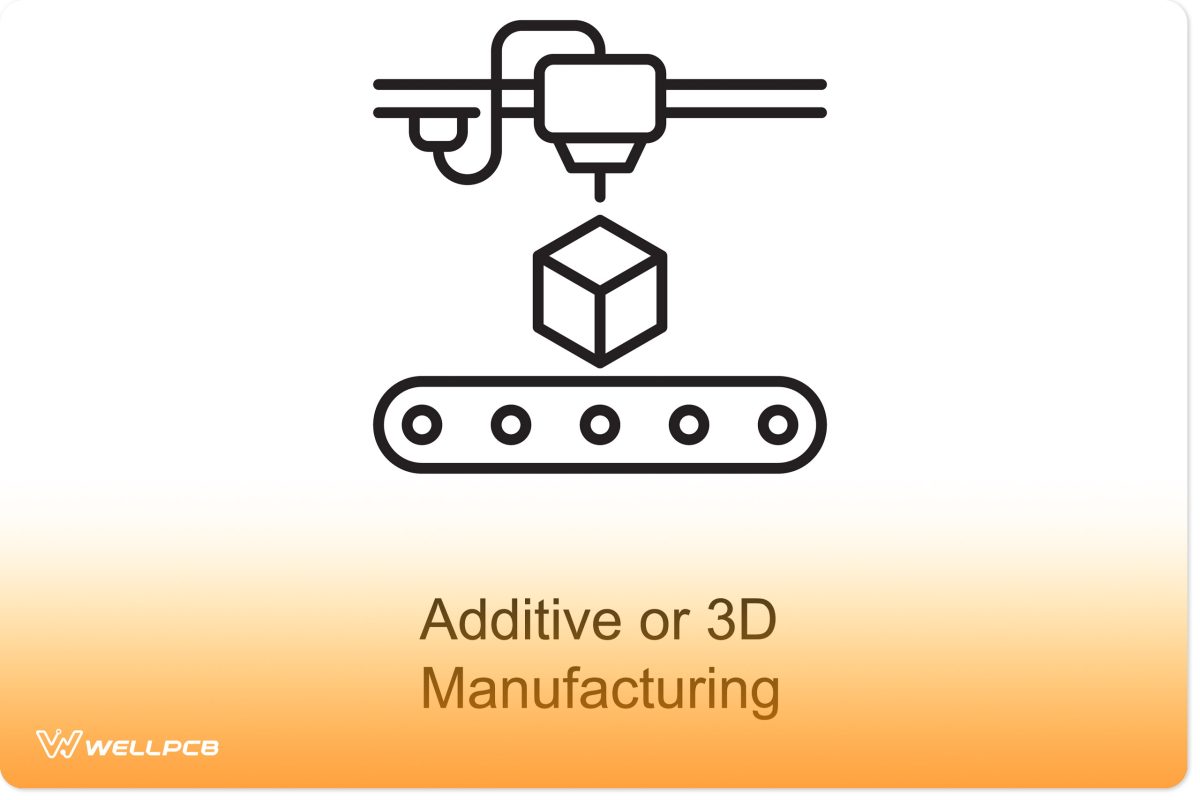
[image: Additive Manufacturing Image]
Additive manufacturing mainly refers to the 3D printing of printed circuit boards. Because it involves a vastly different approach to fabrication than standard PCB manufacturing, it has unique considerations and requirements.
For instance, it requires different materials. Traces for 3D-printed prototype PCBs use conductive inks such as silver nanoparticles. Due to their flexibility, conductive polymers lend themselves well to additive manufacturing, as they can easily be printed layer-by-layer.
This layer-by-layer approach enables designers to create complex trace layouts and patterns easily. However, ensuring that each layer accurately connects can be challenging.
That said, you can overcome it with sensible design choices.
Flexible PCBs
Thin copper traces remain the industry standard for flexible and rigid-flex PCBs. Although emerging materials like graphene and conductive polymers are in the early stages of development, they’re not yet suitable for the mass production of flex PCBs.
Right now, silver and aluminum are the most viable alternatives to copper traces. When designing flexible PCBs, wider traces are important, as they better accommodate bending and withstand mechanical stress.
Either way, your trace width and spacing must conform to the manufacturability rules and guidelines. This will ensure that it can meet PCB manufacturing capabilities.
Keep traces as short as possible and avoid routing them at acute angles for better signal integrity and durability.
Using teardrop-shaped pads at trace-to-pad junctions further improves mechanical stress resistance, resulting in more reliable connections.
Use Expert PCB Assembly Services
When undertaking PCB trace design, going alone is never a good idea. Optimizing the circuitry of your PCB requires the right expertise, consideration, and care. When deciding on your PCB manufacturing partner, it’s best to choose a business with experience and superior customer care.
Making design mistakes while working with complex circuits is almost unavoidable. Contact WellPCB today to learn how we use design rule checks (DRC) to iron out errors and improve the manufacturability of your designs. Choose WellPCB, a service provider that offers a guiding hand.


