

This table elaborates on the different thicknesses of the PCB board used by the designers.
| Weight | Absolute Cu Min. (IPC-4562 less 10% reduction) (μm) [μin] | Maximum Processing Allowance (μm) [μin] | Minimum Final Finish after Processing (μm) [μin] |
| 1/8 oz. [5.10] | 4.60 [181] | 1.50 [59] | 3.1 [122] |
| 1/4 oz. [8.50] | 7.70 [303] | 1.50 [59 | 6.2 [244] |
| 3/8 oz. [12.00] | 10.80 [425] | 1.50 [59] | 9.3 [366] |
| 1/2 oz. [17.10] | 15.40 [606] | 4.00 [157] | 11.4 [449] |
| 1 oz. [34.30] | 30.90 [1,217] | 6.00 [236] | 24.9 [980] |
| 2 oz. [68.60] | 61.70 [2,429] | 6.00 [236] | 55.7 [2,193] |
| 3 oz. [102.90] | 92.60 [3,646] | 6.00 [236] | 86.6 [3,409] |
| 4 oz. [137.20] | 123.50 [4,862] | 6.00 [236] | 117.5 [4,626] |
PCB Trace Thickness
The PCB trace thickness of a PCB board is determined during the design process and plays a critical role in the board’s performance and reliability. Designers commonly select trace thicknesses for four-layer PCBs from standard options, including 0.020″, 0.031″, 0.040″, 0.047″, 0.062″, 0.093″, and 0.125″.
For the inner copper layers, users can choose between ½ oz., 1 oz., or 2 oz. copper foil, depending on the specific requirements of their application.
Figure 1 illustrates how PCB trace thickness varies before and after components are etched into the board’s surface.
Copper thickness plays a vital role in determining PCB thickness. The standard unit of measurement for copper thickness in PCBs is ounces per square foot. For example, 1 oz. of copper corresponds to a thickness of approximately 1.37 mils (thousandths of an inch). This relationship directly affects the electrical performance and design of the board.
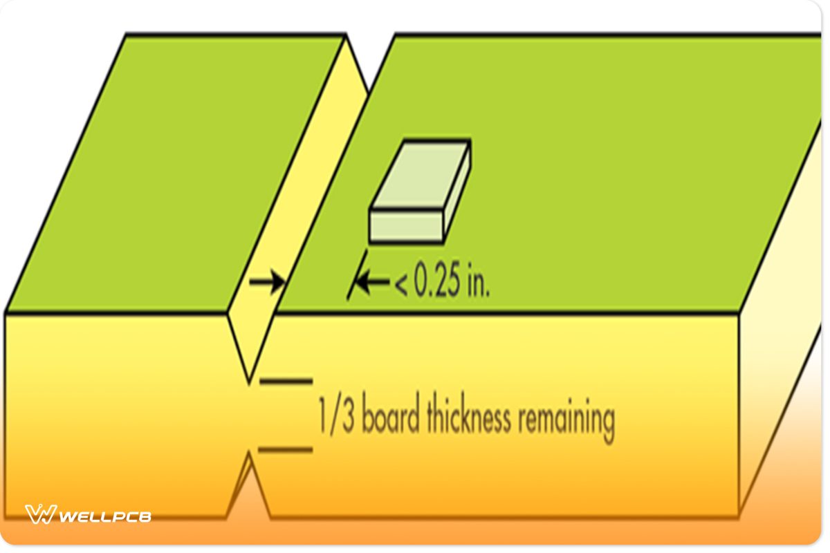
Figure 2 illustrates the relationship between copper thickness, etching depth, and the remaining board thickness, showing how these factors affect PCB design.
FAQ
What is PCB trace thickness?
PCB trace thickness is the thickness of the copper layer on a PCB. It plays a critical role in ensuring efficient current flow and impacts the board’s overall performance and reliability.
How is PCB trace thickness calculated?
PCB trace thickness is calculated using trace width, copper weight, and the current requirements of the circuit. Designers often use calculators or specialized tools to simplify this process and ensure accuracy.
Why is PCB trace thickness important?
Proper trace thickness ensures efficiency, prevents overheating, and improves overall circuit reliability. Incorrect trace thickness can lead to malfunctions, component damage, or reduced performance.
What are the common PCB trace thickness standards?
Typical PCB trace thicknesses include 0.020″, 0.031″, 0.040″, 0.047″, 0.062″, and 0.093″, with the selection depending on the application and design requirements.
How do I choose the right PCB trace thickness?
The right trace thickness depends on your project’s current demands, trace dimensions, and copper weight. Tools like PCB trace calculators can help ensure the correct thickness for your specific design.
Conclusion
The thickness of a PCB is as crucial as the board itself, directly influencing its functionality and performance. Designers perform many complex calculations to determine the optimal depth of the PCB board for the best results.
To simplify this process, designers often use PCB trace thickness calculators to quickly and accurately determine the necessary board thickness. If the PCB trace thickness is incorrectly calculated, it can lead to performance issues or damage the components connected to the PCB.
Designers use precise techniques and accurate calculations to ensure optimal PCB performance while minimizing material waste and preventing overuse. This not only enhances the efficiency of the PCB, but also results in more sustainable manufacturing practices.
WellPCB is your trusted partner for PCB manufacturing, design, and assembly. Visit the WellPCB blog regularly for more practical insights, or contact us for expert guidance to bring your next project to life.
Due to the accuracy of the PCB trace thickness, the material used during the design of PCBs is saved from being wasted or from over-use.