Contents
What is Track Width?

The track, also known as the PCB trace, is the conductive path of a copper layer that connects points on a PCB. Track width refers to the width of this copper trace and is directly proportional to the thickness of the copper track.
Track width is typically measured in millimeters (mm) and plays a crucial role in determining the board’s pattern class. For instance, an ordinary signal layer can transmit efficiently with a track width of approximately 0.150 mm (6 mils).
How to Calculate Trace Width

Using just a few formulas, anyone can determine the ideal PCB trace width. As PCB traces effectively function as resistors, their resistance increases the narrower and longer they are. Below, we’ll show how to calculate trace resistance and deduce the PCB trace width.
First, you should calculate the allowable current using this formula:
I = k * ΔT^0.44 * A^0.725
Where:
- I is the electric current
- ΔT is the temperature change
- A is the track’s cross-sectional area
In order to rewrite the above equation to find track width, we need to make the cross-sectional area the subject of the formula.
Here is the final equation after the rearrangement:
Area[mils^2] = (Current[Amps] / (k * (Temp_Rise[°C])^0.44))^(1/0.725)
Finally, use the resulting cross-sectional area to calculate the PCB trace width with the following formula:
Width[mils] = Area[mils^2] / (Thickness[oz] * 1.378[mils/oz])
Note that these formulas are suitable for tracks carrying 0–35 Amps of current and experiencing temperature changes between 10°C and 100°C.
Track Width Design Tips

Maintaining the correct minimum track width is crucial to ensure your PCB functions reliably. Here are some tips to guide your design process:
- Follow Design Specifications: Always refer to the design specifications and consider the current that needs to pass through the tracks.
- Adhere to the Minimum Track Width Rule: Use a minimum track width of 1.0 mm per amp, ideal for a copper thickness of 1.0 oz/ft², which is standard for most PCBs.
- Avoid Overly Broad Tracks: While ensuring sufficient width, avoid making tracks too broad, as this may interfere with adjacent traces and lead to short circuits.
- Use Track Width Calculators: Track width calculators can help you determine the appropriate width for your specific requirements.
- Consider Copper Thickness: Ensure that the track width is compatible with the copper thickness used in your PCB design.
How to Change Track Width in KiCad
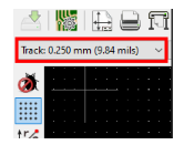
When using KiCad, the popular PCB design software, it’s possible to adjust track width in the settings. To do so, simply follow these steps:
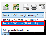
- Open PCBNew: Click on “PCBNew” and select the width-changing dropdown.
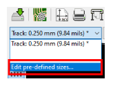
- Edit Predefined Sizes: Select “Edit predefined sizes.”
- Select Track and Vias: In the next window, select “Track and Vias.”
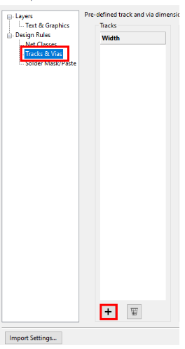
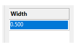
- Add a New Size: Click the + button in the column and enter your desired width (e.g., 0.500 mm).
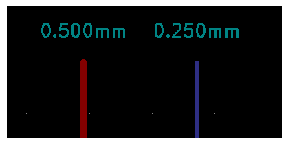
- Confirm Changes: Ensure the new width appears in the dropdown menu. If KiCad reverts to the default 0.250 mm, manually re-enter your desired value.
Note: KiCad occasionally reverts to the default 0.250 mm value. Stay vigilant and adjust the width as needed. Also, compare the Cu-foil thickness in the diagram below to ensure consistency.
Conclusion
This guide has provided an overview of track width and how to calculate it, as well as its importance in PCB design. With this knowledge, you can optimize PCB trace width in your designs to ensure efficient current flow, minimize resistance, and prevent potential PCB failures.
For expert PCB manufacturing services tailored to your precise track width requirements, contact WellPCB today. Our team is ready to help transform your designs into reliable, high-performance solutions.
FAQ
What is PCB track width?
PCB track width refers to the width of the copper traces on a printed circuit board. These traces connect components and play a key role in determining the current-carrying capacity of the board.
How is PCB track width calculated?
PCB track width is calculated using formulas that consider the amount of current, copper thickness, and allowable temperature rise. Track width calculators are often used for quick and reliable results.
What is the ideal track width for power traces?
For power traces, a minimum width of 1.0 mm per ampere is recommended when using a copper thickness of 1.0 oz/ft². This ensures efficient current flow and prevents overheating.