Contents
What Is Laminate in a PCB?
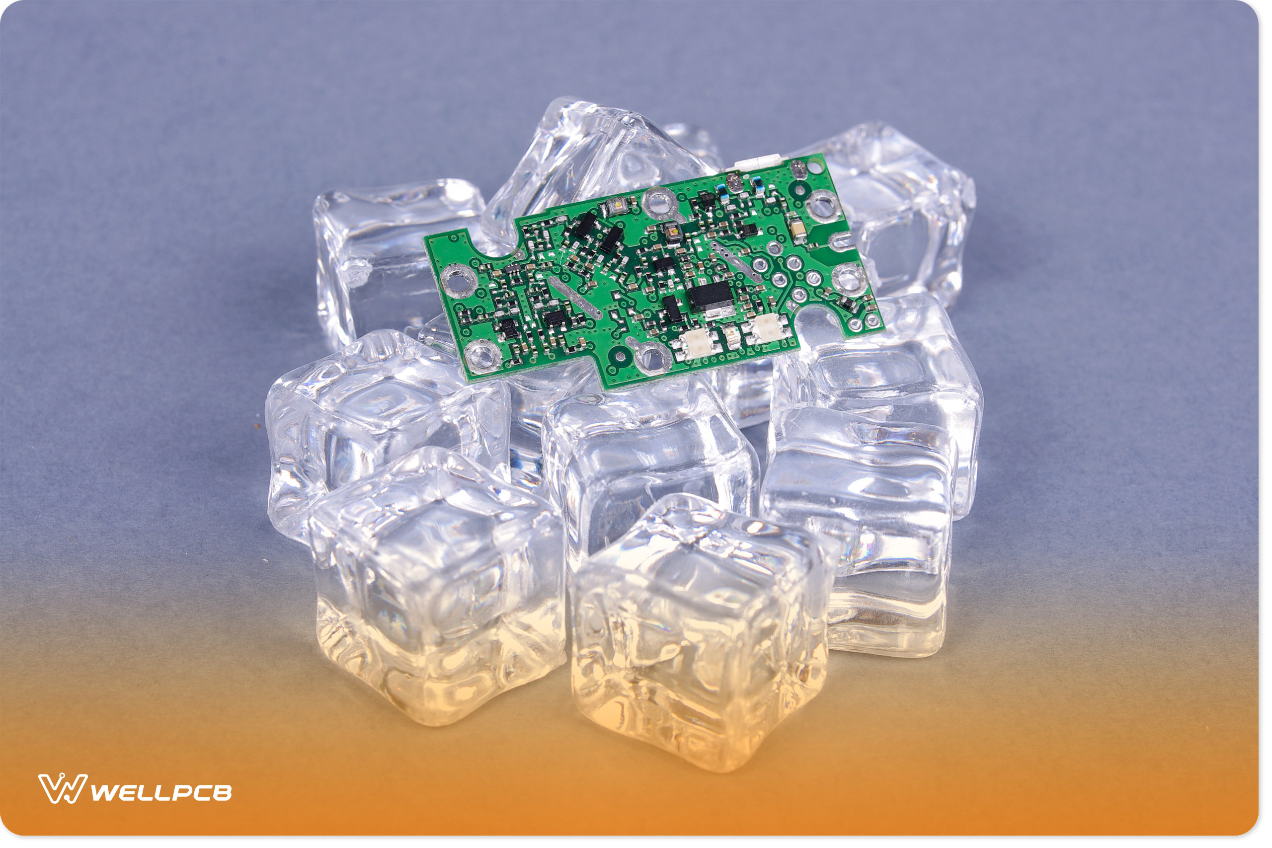
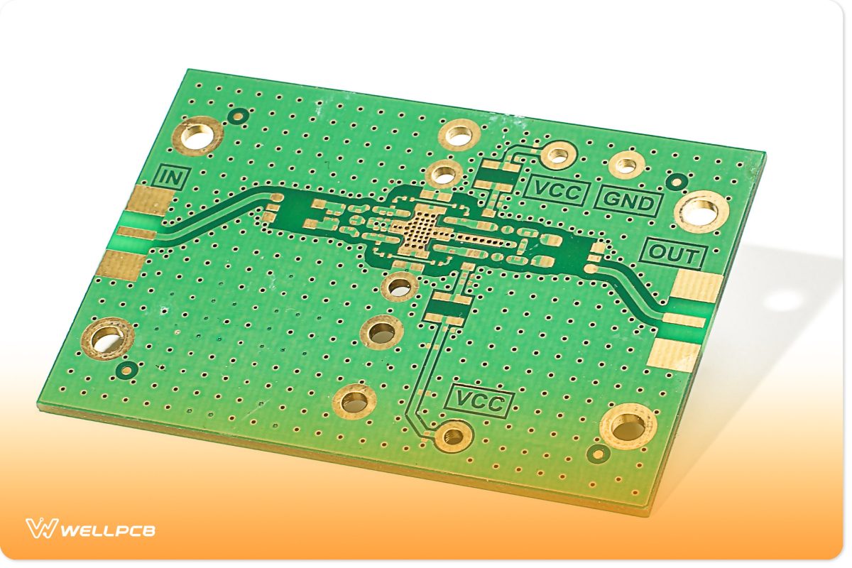
The laminate in a PCB is a simple, thin fiberglass slab that mainly consists of dielectric composite material.
Laminate is required at the beginning of the PCB fabrication process and serves as the board’s foundation once you have your circuit board pattern and design.
Manufacturers create laminates by heating and pressing multiple layers of fiberglass material together using a laminator.
While epoxy resin-impregnated fiberglass isn’t the only material available for laminates, it is the most widely used. This popularity stems from its mechanical strength, thermal resistance, and insulating properties, which help PCB laminates support and secure traces and electrical components.
An effective laminate should allow manufacturers to bond and attach these elements seamlessly. After all, one primary purpose of printed circuit boards is to enable efficient mass production of circuits.
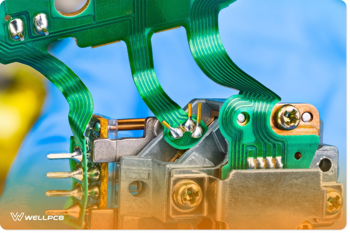
For designs requiring both strength and flexibility, and rigid-flex laminates offer an ideal solution, balancing durability with adaptability for complex applications.
What Are the 10 Types of PCB Laminate Materials?
Some laminate materials are easier to manufacture than others. Here’s why manufacturers use specific products during assembly.
| PCB laminate material | Properties | Benefits | Frequently used in |
| Standard FR-4 | Ideal strength-to-weight ratio, stable at moderate temperatures, flame resistant | Cost-efficient, Reliable under standard conditions, Good electrical insulation | Standard multi-layer PCBs, consumer-grade electronics |
| High TG FR-4 | Glass transition temperature above 170°C, greater moisture and chemical resistance | Withstands higher heat, Suitable for demanding environments, Better longevity | Multilayer PCBs in automotive, industrial, military sectors |
| High IRC TG FR-4 | High insulation resistance, low dielectric constant, high-temperature stability | Minimizes signal degradation, Excellent for high-frequency applications, High performance | High-speed PCBs, telecommunications, RF/microwave printed circuit boards |
| BT-Epoxy | Excellent thermal and mechanical stability, retains bonding strength under heat, good electrical insulation | High bond strength, Excellent thermal stability, Lead-free soldering compatible | Lead-free PCBs, multilayer PCBs |
| Polyimide | Highly stable in extreme temperatures, good flexibility, supports complex circuit designs | Performs well in high-heat environments, Can be used in flexible and rigid-flex circuits, Durable | Rigid-flex and flexible PCBs for aerospace, defense, and automotive |
| Ceramic | Exceptional thermal conductivity, effective electrical insulation, strong mechanical structure | Excellent heat dissipation, Ideal for high-frequency or power applications, Durable under stress | High-power, high-temperature, and high-frequency printed circuit boards |
| Teflon | Low dielectric constant, stable in high-frequency applications, resistant to chemicals and moisture | Perfect for high-frequency applications, Minimal signal loss, Good resistance to environmental factors | RF and microwave PCBs, radar systems, high-performance electronics |
| Metal Core | Perfect for high-frequency applications Minimal signal loss good resistance to environmental factors | Effective thermal management, Supports higher power density, Ideal for heat-sensitive components | Automotive power circuits, energy systems, and high-power LED lighting |
| FR-1 | Fabricated out of phenolic resin and paper, limited to low-complexity applications | Affordable for basic needs, Easy to produce, Suitable for low-demand products | Simple, single-sided printed circuit boards for household and basic electronics |
| FR-2 | Similar to FR-1 but with better electrical characteristics, still based on paper phenolic construction | Cost-effective, Easier to work with than FR-1, Slightly better electrical properties | Single-sided PCBs in low-cost appliances and basic devices |
| CEM-1 | Composed of glass fabric with epoxy resin, better mechanical durability than paper-based materials | Budget-friendly, Better strength than paper-based laminates, Suitable for both sides of the PCB | Single and double-sided PCBs, moderate-performance electronics |
| CEM-3 | Similar to CEM-1 but with a smoother surface, enhanced for automated manufacturing, and slightly higher durability. | Improved mechanical properties, Higher insulation resistance, Better surface finish | Double-sided PCBs for consumer electronics, small appliances |
FR-4
FR-4 (Flame Retardant) is a National Electronics Manufacturers Association (NEMA) designation denoting a class of fire-resistant glass-reinforced materials. The most common is fiberglass sheets bound together with epoxy.
In addition to its compositions, there are certain parameters that laminate material must meet before we can class it as FR-4. For instance, it needs a temperature index of 140 °C and a bond strength greater than a metric ton.
Essentially, materials with these parameters lend themselves well to the production of PCB laminates, and that’s why they’re so prevalent in this regard. These are the main types of FR-4:
- Standard FR-4: The most common FR-4 type. It’s inexpensive, reliable, and mainly used in consumer-grade products like household electronics and devices that don’t face extreme environmental conditions.
- High TG FR-4: A high-performance variant of FR-4. It has a higher glass transition temperature (TG) than standard FR-4. This allows it to maintain its structure at higher temperatures, making it ideal for harsher environments such as manufacturing, military, and industrial applications.
- High IRC TG FR-4: FR-4 materials with a high insulation resistance constant. Thanks to their ability to resist the flow of electrical current, high IRC TG FR-4 materials have the highest performance while being the most expensive. Because they minimize crosstalk and signal integrity degradation, they’re perfect for high-frequency applications like advanced computing and telecommunications.
BT-Epoxy
Much like FR-4, BT-Epoxy laminates are epoxy resin-based. However, unlike most FR-4 materials, they use heat-hardened Bismaleimide-Triazine resin sheets.
The industry sought to create a resin-based material that could perform as well (or even better than) ceramic materials. BT-Epoxy comes near enough to this goal for us to consider it a success.
It outperforms standard and high-performance FR-4 on multiple fronts, especially in its heat tolerance. BT-Epoxy has a lower coefficient of thermal expansion (CTE), higher TG (180 °C), and a higher decomposition temperature (325 °C) than FR-4.
In addition to these properties, BT-Epoxy offers exceptional insulation, low moisture absorption and permeability, and high chemical resistance.
BT-Epoxy is best for multilayer PCBs and is implementable as both a core and prepreg material in HDI builds.
Polyimide
Polyimides are plastic-based (polymer) materials for PCB laminates and other electronics. However, unlike standard plastics, they have a high heat resistance and mechanical strength on par with (and superior to) fiberglass and epoxy-based materials.
With a TG above 300°C, they exceed the performance of BT-Epoxy and FR-4 in this regard. Polyimides are also more tensile and easier to manipulate than other laminate materials, which is why we primarily use them in flex and rigid-flex PCBs.
Due to their exceptional heat, radiation, and chemical resistance, polyimides are well-suited for aerospace, industrial, military, and medical use cases.
Ceramic
Ceramics are a broad class of mostly inorganic materials that you typically find in tiling, roofing, and pottery. However, the ceramic materials we use to fabricate semiconductors and PCB laminates are vastly different. Laminate ceramics are usually metal, oxide, and nitride-based. Some standards consider carbon and silicon to be ceramics, too.
The four most common types of ceramic materials in PCB production are:
- Aluminum Oxide (Al203): Sometimes referred to as alumina. It’s a synthetic material that exhibits strong insulation and high tensile strength. It’s best for high-performance and high-frequency PCBs.
- Aluminum Nitride (AlN): Because of its high thermal absorption, electronics manufacturers commonly use it for heat sinks. Likewise, we can use it to construct PCBs for extremely hot environments.
- Beryllium Oxide (BeO): Sometimes referred to as beryllia. As with many ceramics, it exhibits excellent dielectric properties. However, it’s often avoided because of its toxicity.
- Low-temperature co-fired ceramics: A mixture of ceramic and glass materials. They allow for the direct integration of passive components (built-in PCB components).
Teflon (Polytetrafluoroethylene)
Most people recognize Polytetrafluoroethylene (PTFE) from its use in non-stick cookware and clothing. PCB manufacturers can use PTFE-composites as core material to build high-frequency PCBs.
Due to its non-stick properties, it’s nearly impossible to use pure PTFE as laminate material as it’s difficult to bond with copper. As such, manufacturers typically use Teflon mixed with fiberglass or ceramics to construct printed circuit boards.
Because they can facilitate high signal transmission frequencies (5GHz and above), Teflon-based PCBs are best for radio frequency (RF) applications.
Because of their excellent thermal stability, they perform well in extreme heat and cold alike.
As you may expect, one of PTFE’s greatest selling points is its impressive ability to repel and resist moisture.
It easily resists oil and liquid-based chemicals, making it highly impervious to corrosion.
It’s common knowledge that manufacturing PTFE is incredibly bad for the environment. Perfluorooctanoic acid (PFOA) emissions are released during production, which can be toxic to human and animal health.
Nevertheless, research continues to try to find safer and less impactful ways to create PTFE.
Metal Core
Metal-core PCBs (MCPCBs or metal-backed PCBs) are a class of PCBs that use metal materials as their core. Rather than a laminate material, this describes a type of build.
Most MCPCBs use a three-layer structure, which consists of the metal core layer insulated from the circuit layer by a dielectric layer. The purpose of the metal core is to add extra heat dissipation to the printed circuit board.
Consequently, it typically consists of a material with high thermal conductivity, like aluminum or copper (C110).
It can also be made out of a steel alloy. The dielectric material is usually glass fiber or ceramic-based.
FR-1
FR-1 is a NEMA designation applied to the lowest class of flame-resistant materials. The designation typically denotes materials that use epoxy-impregnated wood fibers like phenolic paper.
It’s one of the least utilized laminate materials due to its low mechanical strength and thermal management.
However, it’s low-cost and exhibits decent flame resistance. This makes it ideal for low-performing single-layer PCBs in educational kits, simple calculators, and low-power LEDs.
FR-2
Much like FR-1, FR-2 is a class of synthetic resin-bonded wood fibers. They’re plastic-reinforced and bonded.
FR-2 materials have a lower Tg (105 °C) than FR-1 (130°C) but are still more mechanically robust. We can use them as an alternative to FR-1 in many of the same low-performance applications. Additionally, they’re also suitable for use in connectors and power supplies.
CEM-1
CEM-1 is a designation describing a class of composite epoxy materials. It uses cellulose wood or paper-based substrate bonded with epoxy synthetic resin. Much like FR materials, CEM-1 materials are flame-resistant.
CEM-1 is substantially cheaper than FR-4. However, it’s not as strong and heat-resistant as FR-4. You can use CEM-1 instead of FR-1 or FR-2, as these materials perform similarly. That said, CEM-1 does display greater tensile strength.
CEM-3
CEM-3 is a higher-grade composite epoxy material. Many consider it a viable alternative to FR-4 because they share a similar composition.
CEM-3 consists of glass cloth combined with epoxy resin and reinforced with glass-fiber padding. This combination produces a thick, solid material with a milky color. CEM-3 has a Tg of 120 °C.
While CEM-3 is substantially cheaper than FR-4, it doesn’t offer the same mechanical robustness or stability. Despite this, it is still used in low-cost PCBs for consumer electronics, communication infrastructure, automotive, and military applications.
What To Consider When Choosing a PCB Laminate Material?
You can judge the value of a laminate by its ability to:
- Provide mechanical support
- Act as a non-conductive substrate
- Maintain signal integrity
- Manage heat (and cold)
- Be manufactured efficiently
- Meet the demands of your budget (affordability)
- Easily available
- Comply with industry standards
- Manufactured and used with minimal impact on the environment
These are some of the properties that we’ve used in the section above to assess the types of laminate materials. In addition to these specifications, you need to consider who your supplier is. Make sure you pick one that offers support and is reputable.
Extra reading: Designing your own printed circuit boards? Learn how to use the sprint layout software tool and get a leading edge with your board designs.
How Does the PCB Lamination Process Work?
The PCB lamination process is complex and comprises several intricate steps. Because of the importance of the laminate material, we, as manufacturers, cannot afford to miss or skip a single step.
Preparation
First, we must ensure that the materials (mainly printed circuit board panels) are contaminant-free. The materials go through cleaning and inspection before we move them on to micro-etching.
Micro-Etching
We use micro-etching to roughen up the surface of the printed circuit board panels. This makes it easier for them to stick together during the lamination process.
Black Oxide Treatment
To further enhance adhesion, we dip the PCB panels in a black oxide solution. This makes it easier for copper to bond to the panels while ensuring they don’t come apart during or after lamination.
In many PCBs, this involves copper-clad laminate, where a layer of copper is bonded to one or both sides of the dielectric material to serve as the conductive surface for circuits.
Arrangement of the Inner Layers and Stack-Up of the PCB
Next, we must sort the various panels into the correct order. They begin with the inner layers and then the outer prepregs, which sit between the copper foils and the core material.
Once we’ve finalized the stack-up, we lightly bond all the layers with a glue machine. This ensures that the layers remain aligned during lamination.
The construct then undergoes pre-pressing to remove any air pockets and prepare it for lamination.
Lamination and Demolding of the Panels
The next step is to place the combined sheets into a PCB laminator. The lamination machine works by heating and pressing the sheets together.
As the heat increases, the resin from the prepreg begins to liquefy and flow into the inner layers. It’s crucial that the PCB laminator increases the temperature and pressure gradually to ensure bonding is even. This curing process can take up to two hours.
Once complete, the PCB laminator slowly releases the pressure and turns the temperature down. After lightly inspecting the PCB for any deformities, we move the board to the cold press to ensure that it’s stable.
Then, we inspect and deburr the board by removing any additional mold or material from the sides and corners.
Hole Registration and Completion
Lastly, we perform a final inspection of the board using an x-ray machine. This enables us to perform a hole registration where an inspector verifies that any holes in the PCB align accurately. The holes then undergo smoothing to remove any rough or uneven edges.
Make the PCB Assembly Process Easy
While there are a multitude of PCB laminate materials and types, you don’t have to stick to one for your PCB stack-up.
For instance, some materials work better for cores, while others are best suited for outer build-up layers.
By this logic, you could potentially use a BT-Epoxy prepreg with a high-performance FR-4 core.
Complex constructions of this nature require deft hands, and not all manufacturers have the expertise to deliver these designs.
To get the most from your printed circuit boards, it’s crucial to partner with an experienced and reputable manufacturer who can meet the fabrication demands of your laminates.
Need help choosing the right PCB laminate material? Contact WellPCB for expert guidance.
We’re widely known as the cheapest PCB manufacturer and can help cut material costs and make your designs a reality.