Contents
- 1 What is PCB Cross-Section Analysis?
- 2 The Basics of PCB Cross-Section Analysis
- 3 Multilayer PCBs
- 4 Tools for PCB Cross-Section Analysis
- 5 PCB Trace Cross-Section Geometry
- 6 Cross-Section Test Coupons and Inspection Criteria
- 7 Preparing and Using Test Coupons
- 8 Challenges in the Cross-Section Preparation of Vias and PTHs
- 9 Why is PCB Cross-Sectional Analysis so Important?
- 10 Conclusion
- 11 FAQ
What is PCB Cross-Section Analysis?
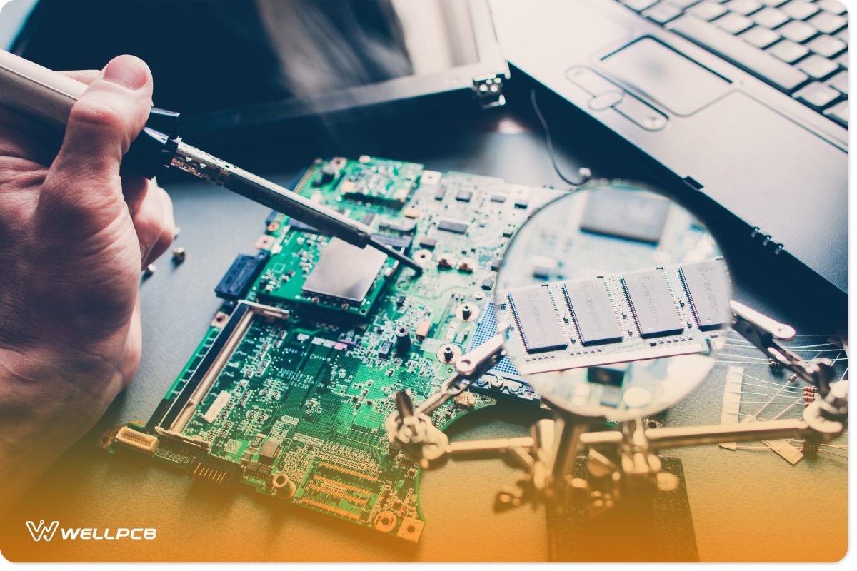
PCB inspection can be classified as either destructive or non-destructive. This is similar to the difference between an X-ray and a biopsy or autopsy in medical analysis.
Cross-section analysis is a destructive method that involves a section of the PCB being physically removed for detailed material inspection.
PCBs are composed of various materials and components, and failure in a single element can jeopardize the entire system. Cross-sectioning (or microsectioning) allows us to evaluate the quality of the PCB’s internal mechanisms in order to identify potential faults.
The Basics of PCB Cross-Section Analysis
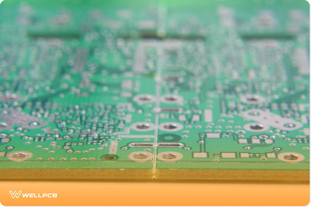
To perform cross-section analysis, you must microsection a portion of the PCB. This involves isolating and extracting the defective region as precisely as possible, often using tools like schematics or thermal imaging for guidance. The extracted piece can then be analyzed to uncover the root cause of failure.
PCB Core Cross-Section
Once the PCB core cross-section has been isolated and separated, it is encased in potting material to protect it during polishing.
Once mounted, the cross-section is ground to reveal the desired plane of interest using silicon carbide paper, colloidal silica, or aluminum powder.
Heavy Copper PCBs
Heavy copper PCBs are designed for industrial and heavy-duty applications in harsh environments. These PCBs offer benefits such as enhanced thermal resistance, reduced risk of circuit failure, and increased current-carrying capacity. Cross-section analysis helps ensure heavy copper PCBs function as intended.
Multilayer PCBs
Multilayer PCBs are essential for compact designs, enabling components to be densely arranged. They feature numerous vias and holes connecting layers. They feature numerous vias and holes connecting layers.
Solder Joint Cross-Section Analysis
Solder joints are prone to issues like open joints, solder skips, and hidden component damage. This is often due to premature hardening during the soldering process.
Microsectioning a solder joint reveals critical information about defects and enables the assessment of solder thickness and intermetallic compounds.
Tools for PCB Cross-Section Analysis
Cross-section analysis requires specialized tools and equipment, particularly in the polishing and observational phases. This section highlights the key tools used in the microsection analysis process.
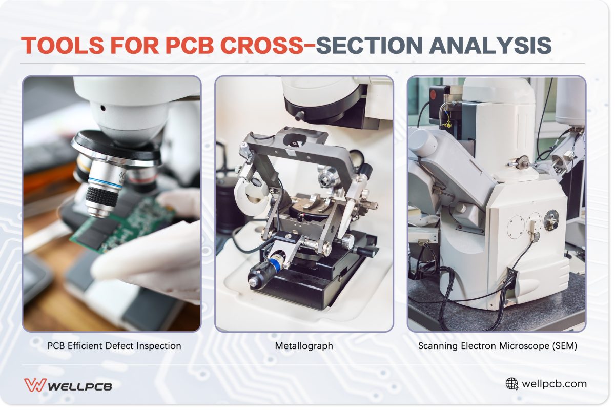
Metallograph
A metallograph is an optical microscope designed for metallography and is a critical tool in PCB cross-section analysis. Typically equipped with a camera, it enables the capture of high-resolution images of the PCB’s cross-section.
Cross-sectioning is sometimes known as metallographic preparation. The metallograph offers zoom of up to 1000x, allowing for extremely detailed inspections. The device is instrumental in finding defects within the cross-sections.
Scanning Electron Microscope (SEM)
A Scanning Electron Microscope (SEM) uses a focused electron beam to create highly detailed images of PCB cross-section surfaces, with magnification ranging from 10x to 2000x. This makes it possible to extract valuable information about a sample’s composition.
The interaction between the electron beam and the atoms in the PCB cross-section produces various detection signals, including: secondary electrons, back-scattered electrons, characteristic X-rays, light cathodoluminescence, absorbed current, and transmitted electrons.
A significant advantage of using an SEM is that it does not require the PCB cross-section to be polished before inspection. Using the SEM’s back-scattered electron mode, it is possible to extract the specimen’s basic compositional and topographical information.
Efficient Defect Inspection
Micro- and cross-sectioning serve as useful techniques for failure analysis, as they can identify causes of internal errors. Issues such as over-etching, poor soldering, and faulty pads are among the problems that cross-section analysis can detect through detailed optical inspection.
This process provides a visual means to identify and resolve fabrication issues, ensuring product quality. For customers, it’s crucial to understand the extent of their PCB manufacturer’s testing and quality assurance practices to ensure reliable results.
PCB Trace Cross-Section Geometry
PCB cross-section geometry describes the spatial shape and alignment of a PCB’s components. A full cross-section geometry illustrates the relationship between the PCB’s layers, material, components, and traces.
Specifically, trace cross-section geometry refers to the spacing and alignment of traces. These diagrams often represent the routing and differential impedance of the traces. The most common cross-sectional geometries are coplanar, microstripline, and stripline, each with inherent variations suited to specific design requirements.
Cross-Section Test Coupons and Inspection Criteria
Under IPC 6012, customers typically specify the inspection criteria for cross-section analysis. This section explains test coupons and the inspection criteria used for evaluating PCBs.
Test Coupons
Cross-section analysis doesn’t require a PCB to fail before testing. Test coupons allow for destructive testing while preserving the main functionality of the board. These coupons are fabricated as extensions of the PCB, and designed for easy removal without affecting the board’s operation.
The test coupons are made from the same material and share the same specifications as the original PCB, including trace width, copper composition, and via patterns. They are typically placed at least one inch from each end of the PCB. After removal, the extensions are encased in a polymer to form a sample, often referred to as a puck due to its shape.
The puck is then ground down to expose the interior region of interest. Once the plane of interest is revealed, experts inspect it using a metallograph or SEM. Test coupons are designed to comply with IPC 2220 standards, ensuring consistent and reliable analysis.
Given the complexity of PCBs, different types of test coupons are created to analyze specific regions or components. This helps to identify issues such as trace defects, poor soldering, or layer misalignment.
Through Hole Coupons
Through-hole coupons are used to assess solderability, solder masks, legend inks, and similar characteristics. However, since cross-section analysis is destructive, each test coupon can only be used once, rendering it unusable after the assessment.
Assessments
Cross-section assessments focus on critical PCB components and features, including plated through holes, vias, and barrel walls. The quality and structure of barrel walls can also easily be assessed, along with the quality of copper plating, thickness, and voids.
Preparing and Using Test Coupons
Before placing a test coupon under a microscope, it needs to be prepared properly.
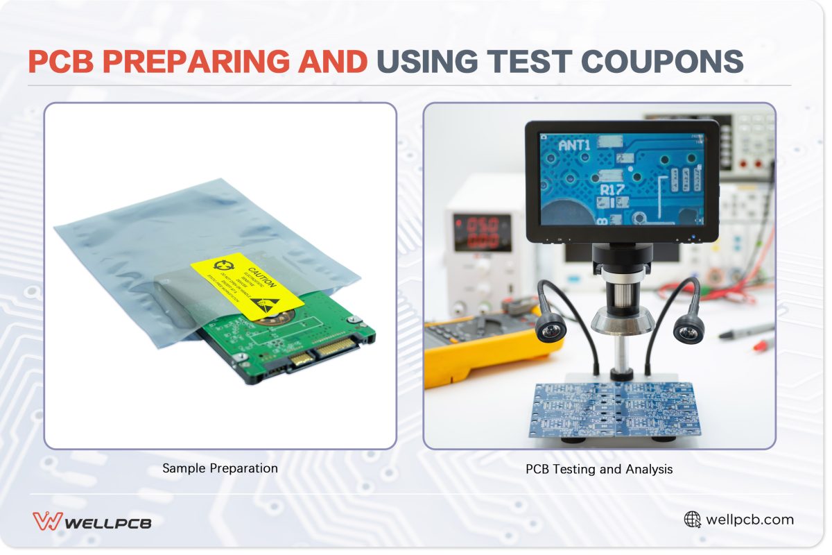
Sample Preparation
The preparation process begins by labeling the coupon according to its position and orientation on the PCB. For instance, left-bottom coupons may be labeled as LBC, right-top as RTC, and horizontal coupons as HC. These labels help with sorting and identifying the samples.
After labeling, the coupons are extracted from the PCB using a diamond saw. Once separated, they are cleaned with deionized water in an ultrasonic cleaning system to remove any contaminants.
Next, the coupons undergo micro-etching to enhance surface details before inspection and digital photography. If any faults are discovered in the captured images, the specific regions are magnified for closer examination, and observations are recorded.
During this process, we also measure critical parameters including dielectric thickness, solder plating thickness, and copper thickness (basic, plating, and total thickness).
Analysis Process and PCB Cross-Section Results
The primary goal of cross-section analysis is to identify flaws resulting from the fabrication process. This helps us refine the fabrication process and prevent similar defects in future production.
While non-destructive testing methods like thermal testing can detect certain issues, they are often insufficient for identifying subtle flaws in the PCB’s structure.
For example, breaks in the solder joints or microscopic defects may go unnoticed without destructive testing.
Cross-section analysis offers a deeper view of the PCB’s makeup, revealing critical details such as solder grains, metals composition, cracks, and voids.
Challenges in the Cross-Section Preparation of Vias and PTHs
Given their delicate structure, preparing vias or plated through holes (PTHs) for cross-section analysis presents a few challenges. Maintaining the integrity of the vias during preparation is critical for accurate measurement and evaluation.
For instance, the polishing process must ensure that the final product closely reflects the original via structure. Scratches also need to be carefully avoided, as they can obscure critical details and lead to inaccurate analysis. Proper alignment during the potting phase is essential in order to maintain the sample’s accuracy.
Careful and skilled polishing is also required to remove defects while avoiding edge rounding, which can distort the true dimensions of the via or PTH.
Why is PCB Cross-Sectional Analysis so Important?
PCB cross-sectional analysis plays a crucial role in evaluating the following aspects of PCB design and fabrication:
- PCB core materials
- Build quality in multilayer boards
- Solder-mask thickness
- PCB surface finish
- Quality of connections between layers
- Integrity of pads
- Thickness of hole-wall plating
- Via and via fill
Manufacturers may conduct micro-sectional analysis at various phases of the fabrication process:
- After drilling to inspect hole quality and registration accuracy
- After plating to observe wrap and barrel thickness
- During the final quality check to identify remaining defects, measure overall thickness, and assess plating quality
By performing cross-sectional analysis at multiple stages, manufacturers can identify and address potential issues early in the production process.
Conclusion
Cross-section analysis is one of several quality control techniques used by PCB manufacturers. As a destructive testing method, it provides detailed insights into subtle defects that other non-destructive methods may miss.
This technique involves cutting a PCB into smaller samples for thorough inspection and evaluation. It helps ensure the reliability and performance of the final product, making it a critical step in PCB quality assurance.
We hope this guide has provided a clear understanding of why and how PCB manufacturers perform cross-section analysis.
If you’re looking for expert PCB manufacturing services with rigorous quality testing, contact WellPCB today. Our team is ready to help you achieve the highest standards for your PCB projects.
FAQ
What is PCB cross-section analysis?
PCB cross-section analysis is a destructive testing method used to inspect the internal structure of a PCB. It involves analyzing a cross-sectional sample to detect flaws such as cracks, voids, and solder defects.
What equipment is used in PCB cross-section analysis?
The equipment commonly used includes metallographs, scanning electron microscopes (SEM), and efficient defect inspection tools.
Why is cross-section analysis important?
Cross-section analysis is vital for ensuring build quality, identifying defects, and validating the integrity of core materials in multilayer PCBs.