Capabilities
WellPCB is focusing on online prototype orders to meet the requirements for High Quality, Low Cost, Fast Delivery, Easy Ordering from customers around the world. We can accept 4 kinds of files format (Gerber, .pcb, .pcbdoc or .cam file format) for PCB Prototype Manufacturing.
We perform full DRC checks of all Client files and inform you immediately if we find any problem. We then will work with you to correct the files, so they are suitable for manufacturing. Please check our capability overview below for reference. Please contact us if you have a special requirement not listed in the following table.
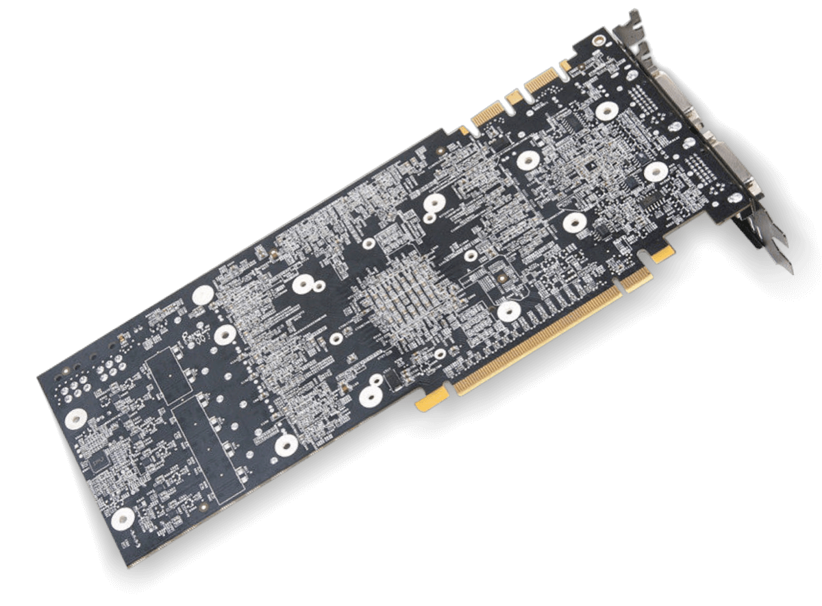
Rigid pcb

We can accept 4 kinds of files format (Gerber, .pcb, .pcbdoc or .cam file format) for PCB Prototype Manufacturing. We perform full DRC checks of all Client files and inform you immediately if we find any problem.
We then will work with you to correct the files, so they are suitable for manufacturing. Please check our capability overview below for reference. Please contact us if you have a special requirement not listed in the following table.
-
Layer Counts1-32 Layers
-
Lead TimeNormal: 5-6 Days
Expedited: 24-48Hours -
MaterialsFR4, High TG FR4, Halogen Free material, CEM-3, Rogers HF material, etc.
-
Finished Copper Thickness0.5 - 5 OZ
-
Finished Board Thickness0.2 - 6.0mm
-
Min. Line/Track Width&Space3mil
-
QualificationsISO 9001:2008, ISO14001:2004,
ISO / TS 16949:2009
UL Certified -
TechnologyOn-Across Blindried Vias, Characteristic Impedance Control, Rigid-flex Board etc
-
Solder Mask ColorGreen, Black, Blue, White, Red, Yellow, and Matt, etc.
-
Legend/Silkscreen ColorWhite, Yellow, Black, etc.
-
Surface TreatmentLeaded HASL, Lead Free HASL, Immersion Gold, OSP, Immersion tin, Immersion Silver, etc.
-
Wrap and Twist≤0.7%
-
Other TechnologyGold Finger, Peelable Mask, Non-across Blind-Buried vias, Characteristic Impedance Control, Rigid-Flex Board etc.
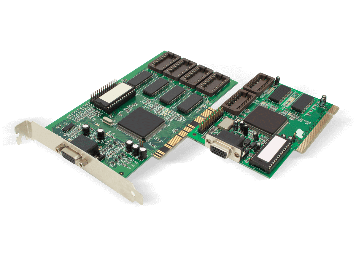
pcb ASSEMBLY
We strive to make the whole assembly process as easy as possible:
Single Point Source: No need to order bare board PCB from one supplier, solder stencil from another supplier, and PCB assembly from yet another supplier.
We provide prototype promotions and also mass quantity production from one board to thousands of boards.
We offer a rapid turnaround, kit service, turnkey service, harness assembly, and box build service.
-
Placer Speed600,000 Chips/Hour
-
Lead Time25+ Days (To Be confirmed)
-
SMT
-
PCB Size50mm×50mm ~ 610mm×508mm
-
PCB Thickness0.5mm ~ 4.5mm
-
Min. Diameter / Space of BGA0.2mm / 0.35mm
-
Minimum Width / Space of QFP0.15mm/0.25mm
-
QualificationsISO 9001: 2008
-
Accuracy<±30µm, Under the Condition of 3σ, CPK≥1
-
Reliability TestFlying Probe Test/Fixture test, Impedance Test, Solderability Test, Thermal Shock Test, Hole Resistance Test, and Micor Metallographic Section Analysis, etc.

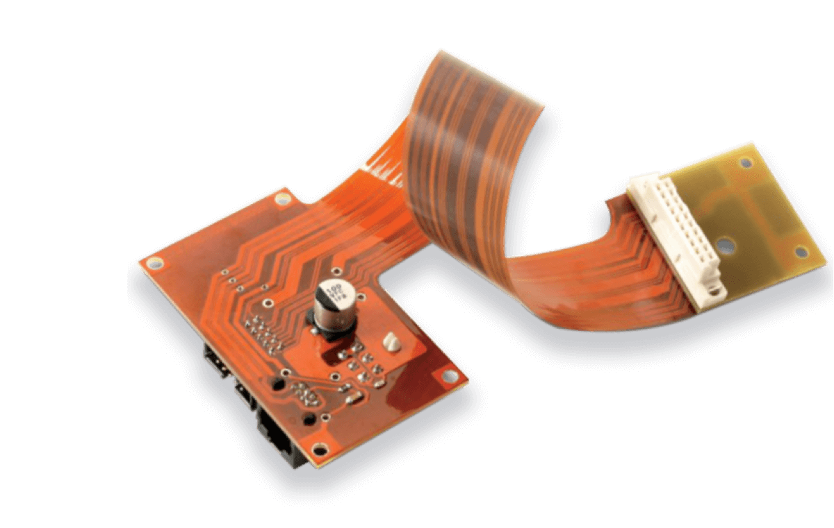
FLEX pcb

Manufacturing Capability:Conventional Capability
Ultimate Capability:Unconventional ability;Submit to review beyond these Capabilities.
-
FPC Base Material(Adhesive)ShengyiSF302:PI=0.5 mil,1 mil,2 mil;Cu=0.5 oz,1 oz
ShengyiSF305:PI=0.5 mil,1 mil,2 mil;Cu=0.33 oz,0.5 oz,1 oz -
FPC Base Material(Adhesiveless)SongxiaRF-775/777:PI=1 mil,2 mil,3 mil;Cu=0.5 oz, 1 oz (Ultimate:PI=1 mil,2 mil,3 mil;Cu=2 oz)
Xinyang:PI=1 mil, 2 mil;Cu=0.33 oz, 0.5 oz, 1 oz
Taihong PI=1 mil, 2 mil;Cu=0.33 oz, 0.5 oz, 1 oz
Dubang AP:PI=1 mil, 2 mil, 3 mil, 4 mil;Cu=0.5 oz, 1 oz (Ultimate:PI=1 mil,2 mil,3 mil,4 mil;Cu=2 oz) -
Layers1-4 Layers (Ultimate:5-8 Layers)
-
Thickness of Finished Product (Flex Part,No Stiffener)0.05-0.5 mm (Ultimate:0.5-0.8 mm)
-
Size of Finished Products (Min)5 mm*10 mm (Bridgeless); 10 mm*10 mm (Bridge)
Ultimate:4 mm*8 mm (Bridgeless); 8 mm*8 mm (Bridge) -
Size of Finished Products (Max)9 inch*14 inch
Ultimate:9 inch*23 inch (PI≥1 mil) -
Impedance ToleranceSingle-Ended:±5Ω(≤50Ω),±10%(>50Ω)
Ultimate:Single-Ended:±3Ω(≤50Ω),±8%(>50Ω) -
Impedance ToleranceDifferencial:±5Ω(≤50Ω),±10%(>50Ω)
Ultimate:Differencial:±4Ω(≤50Ω),±8%(>50Ω) -
Tolerance of Finger Width±0.1 mm (Ultimate:±0.05 mm)
-
Min Distance to the Edge of Finger8 mil (Ultimate:6 mil)
-
Min Distance between Pads4 mil (Ultimate:3 mil)
-
Minimum Laser Hole0.1mm
-
Minimum PTH0.3mm
-
Min NPTH Tolerance±2 mil (Ultimate +0, -2 mil or +2 mil, -0)
-
Solder Bridge Min Width(Bottom Copper<2OZ)4 mil (Green), 8 mil
-
Solder Bridge Min Width(bottom copper 2-4OZ)<2OZ)6 mil, 8 mil
-
Overlay Colour<2OZ)White, Yellow (Printed Character: White)
-
Type of Surface Treatment<2OZ)OSP HASL, Lead Free HASL, Immersion Gold, Hard Gold, Immersion Silver, OSP
-
Selective Surface Treatment<2OZ)ENIG+OSP, ENIG+G/F
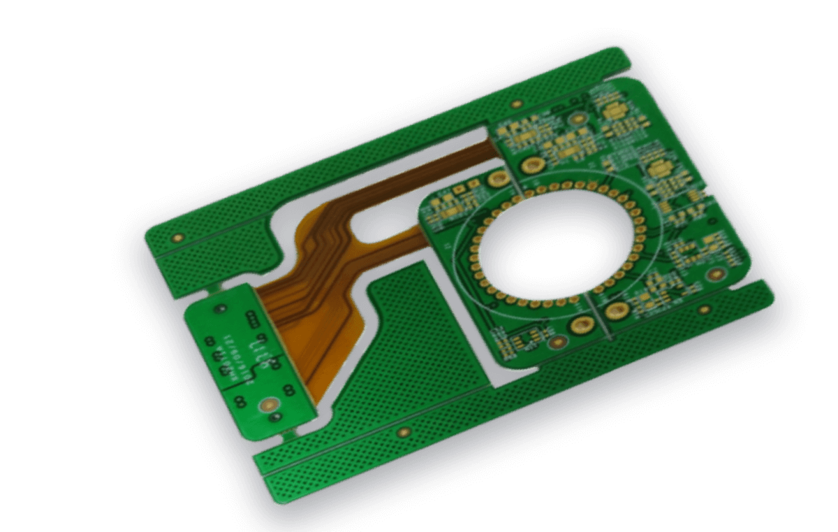
rigid-FLEX pcb

We serve our customers with strong technical R&D capability, various products, and stable and quick delivery capability. We are one of the competitive companies in the domestic with the high-class level in rigid-flex board fields.
Please check our capability overview below for reference. Please contact us if you have a special requirement not listed in the following table.
-
FeatureCapability
-
MaterialPolyimide Flex+FR4
-
Solder Mask Color(Rigid Part)Green, Red, Yellow, Blue, White, Black, Matte Black, Matte Green, Matt Blue
-
Covrelay Color (Flex Part)Yellow Coverlay, Brownish Yellow
-
Silkscreen ColorWhite, Black, yellow
-
Via ProcessTenting Vias,Plugged Vias,Vias not Covered
-
Max Panel Size406mmx736mm
-
Min Panel Size10mm*15mm
-
Min. Track/Spacing3.5mil/ 4.0mil
-
Min. Hole Size0.15mm
-
Rigid-Flex Thickness0.2-4.0mm
-
Impedance Control ToleranceSingle-ended:±3Ω(≤50Ω),±5%(>50Ω)
Differential Pair:±3Ω(≤50Ω),±5%(>50Ω) -
Twist & Warp min.0.75%(Symmetrical)
1.5%(Symmetrical -
Adhesive dispense width1.5±0.5mm(Slot Width≥10mm)
-
Min Distance Between R-F Connect Area to Conduct0.3mm(Half Depth Slot Process)
0.5mm Normal -
Min. Width of Resin Flow Out in R-F Connect Area0.5mm
1.0mm Normal -
Max inner Layer Finished Copper Thickness3oz
-
Min Mechanical Drill Size0.15mm (<=1.6mm)
0.2mm (<=2.5mm) -
Min Half-Hole (pth) Size0.3mm
-
Laser via Size4mil-6mil(Advance 6mil
-
Max buried Hole Size0.4mm
-
Max Drill Hole Size6.3mm
-
Max A/R for Through Hole12:1
-
Max A/R for Laser Blind Hole0.8:1
-
Outline Tolerance±0.1mm