Contents
- 1 Reasons as to why Gold-Plating Is a Necessity for Gold Fingers
- 2 Common Materials Used in the Production/Manufacture of Gold Fingers
- 3 Limitations of Gold Finger Technology
- 4 Basic Applications of Gold Fingers
- 5 Edge Connector: What is it?
- 6 Edge Connector Beveling
- 7 Guidelines, Standards & Regulations guiding Gold Fingers
- 8 Conclusion
Reasons as to why Gold-Plating Is a Necessity for Gold Fingers

PCBs’ connection points are primarily subjected to constant unplugging and plugging based on the nature or role of interconnecting PCBs. Therefore, if there is no durable contact edge, then this means that they are prone or subject to wear and tear that may bring about device malfunction.
The habit of using gold to plate a majority of connectors helps prolong the durability of edge connectors. But isn’t gold too expensive of all the metals out there? Other metals, such as copper, can work fine, but gold is preferred based on plenty of advantages that it offers.
Gold has always been preferred over other metals since it has proven to be highly corrosive resistant and consists of high electrical conductivity. Better yet, gold can be easily alloyed with nickel or cobalt to increase further its ability to withstand wear and tear after a short time.
There have been earlier experiments undertaken to find out the resistance of gold compared to other metals, and gold has been shown to have one of the lowest resistance levels compared to other metals. Better yet, gold has also been found to be highly inert and does not oxidize or immediately react with other metals.
Common Materials Used in the Production/Manufacture of Gold Fingers
Have you ever asked yourself what kind of materials you require to manufacture gold fingers for edge connectors? Probably not. You get gold fingers from flash gold. Flash gold is known as one of the hardest gold.
It is important to note that the specifications needed to manufacture gold fingers have to be completely precise. There should be room for error as such may cause the whole device to operate poorly or fail to perform at all.
Again, the thickness has got to be in the range of around 3Us to 50Us. Unlike other materials in abundance, flash gold has turned out to be one of the most popular materials to use based on its high level or standard of the harness that ensures it comes with a long working life that will not require constant repair.
Flash gold is a material known to survive plenty of insertion or actuation forces and removal that can go up to 1,000 and above. Additionally, flash gold is very easy to solder, unlike other materials known to be tough.

Limitations of Gold Finger Technology
Gold finger technology is of great importance. But sadly, its application remains limited due to several reasons. For instance, plated pads have to be on the edge of the PCB. Since gold plating requires an electroplating process, there has to be a connection that links the plated pads and the panel frame.
Most plating pads manufactured by players in the industry produce fingers that do not exceed over 40mm. If you require longer or oversized gold fingers, then the process of creating them will intensify.
The above is not all. If you don’t know, the inner layers of the edge connectors must be free of copper material. Otherwise, the entire process/steps of beveling the contacts can expose the copper material.
Apart from flexible printed circuit boards, when gold-plating on both sides of the PCB, the least separating distance between the lower and the upper layers of the printed circuit board is supposed not to exceed 150mm, while the maximum length should not be more than 40mm.
There are other rare cases where gold fingers appear shorter or longer than the rest. It means that the shorter pads will not fail to be connected vertically to the plating bar, an aspect that may go ahead to affect matters to do with functionality.
Basic Applications of Gold Fingers
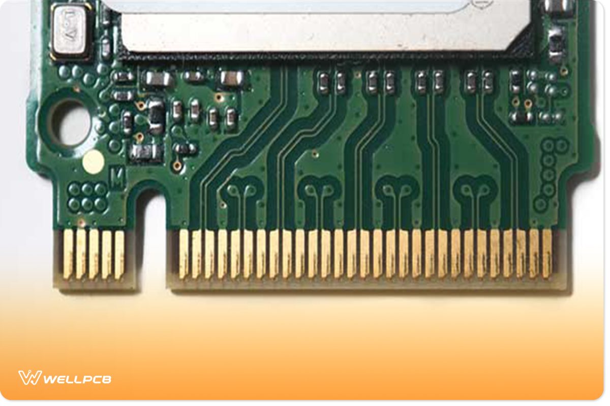
It is common to find Gold fingers as the primary connecting contact between two adjoining printed circuit boards. Besides its conductivity, the gold’s primary purpose is to shield the connecting edges from instances of wear and tear due to its many uses.
The functions that gold fingers play are quite many. However, there are those basic applications with some of the many uses of gold fingers, including the following commercial and technical applications:

• Edge Connector Beveling—Special adapters: Among other things, gold fingers make it easy to include or add several enhancements to a PC.
• Interconnection points: if a secondary PCB connects to the motherboard, several female slots such as ISA, AGP, or PCI slots will suit in place. Gold fingers conduct signals between the computer, a peripheral device, or even an internal card through such slots.
• External connections: gold fingers provide external connecting contacts, especially computerized industrial applications/machinery.

Edge Connector: What is it?
A printed circuit board consists of a part known as an edge connector. You can find it on the edge of a PCB board that gets plugged into the matching socket of a computer or any other device. An edge connector usually has full metallic tracks applied toward the output of the electrical connection.
Edge connectors are used mainly across electronic components, especially in peripheral technologies and computers. There are many advantages associated with them, some of them being that they are cost-effective, robust, simple, and highly durable. Additionally, they are highly reliable to meet the required standards.

Edge Connector Beveling
Beveling is the process of reducing or minimizing a square edge on a given object to achieve a sloping side. On a PCB, edge connector beveling, especially in gold finger plating, is undertaken after the solder mask and moments before initiating the surface finish.
Edge connector beveling is done to connectors to make sure that you achieve insertions quickly. Without such, inserts may not be easy to achieve. In most cases, beveling is done or undertaken based on the specifications of the client.
In most cases, the bevel is made at angles of around 30 to about 45 degrees. Some circuit boards have longer gold fingers, and you have to bevel them to fit together as one complete piece. Still, other devices need edge connectors of specific measurements, an aspect that makes beveling a necessity.
It is necessary to bevel the edge connector to ensure that the fingers snap together into place with a lot of ease, failure to which parts of an edge connector may fail to fit with each other.
Guidelines, Standards & Regulations guiding Gold Fingers
Some of the most common standards that act as a guide towards the production of gold fingers meant for PCBs are those published by The Institute for Interconnecting and Packaging Electrical Circuits.
The above organization later changed its name to The Association for Connecting Electronics Industries, and way back in 2002, it released several standards that pertain to gold fingers. Some of the essential guidelines for the manufacture of gold fingers include:
Finishing size and thickness – layers of the gold fingers must be measured to ensure that the thickness range is between 3u and 50u.
Inspection of contact edges visually – the edges have to be very clean, simple, and smooth under simple visual investigation.
Chemical composition – gold used here must contain at least 10% of cobalt.
Tape testing of contact edges – this test is required to establish the adhesiveness of gold fingers.
Conclusion
Gold finger PCBs play quite an integral part in plenty of electronic devices. Gold plating is currently one of the most widely adopted technology. As mentioned earlier, the reasons why gold is the preferred material are quite many, chief among them being that gold doesn’t corrode, oxidize, and last for long. While certain limitations accompany this technology, gold plating, especially for edge connectors, comes with many advantages that you cannot ignore. Better yet, several guidelines guide the production of gold finger PCBs to ensure the maximum protection of customers from faulty products. Through this guide, you’ve mastered quite several essential aspects regarding gold finger PCBs, especially in edge connectors. With such knowledge, you have a chance to choose the best gold finger PCB.


