Contents
- 1 What is a High Current PCB?
- 2 High-Power PCB Design Guidelines
- 2.1 Trace Width and Thickness
- 2.2 You Don’t Need Solder Masks
- 2.3 Copper Bars Work for Very High Currents
- 2.4 Isolate Heat-sensitive Components
- 2.5 Short Traces Work Best
- 2.6 Multiple Layers and Traces? Use Via Stitching
- 2.7 Internal Layers can Create High Current Paths.
- 2.8 High-current components need Polygon Pours.
- 3 Tips to Improve Your High-Current PCB’s Layout Effectiveness
- 4 Benefits of High Current Heavy Copper PCBs
- 5 Final Thoughts
What is a High Current PCB?
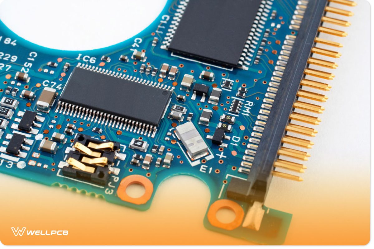
Electronic Circuits
There’s a tool for every task or application—the same goes for high-current PCBs. These circuit boards are the go-to for high-current applications.
While there’s no specific definition for high-current PCBs, we could say they are circuits that work with components that produce high currents.
These high-current boards possess specialized features that make them durable and resilient enough to handle currents beyond the regular amps.
However, these circuits may pose design problems, especially for beginners. Indeed, there are several things to note when designing them. If you don’t consider these factors, you’ll end up with design failures and faulty circuit operations.
Sounds tough? Don’t worry! We’ll go through the basics in the next section of this article.
High-Power PCB Design Guidelines
As we previously mentioned, there are several things to consider when designing high-current PCBs. These factors are the basics you need to know before starting your designs.
Now, let’s take a closer look at these design guidelines.
Trace Width and Thickness
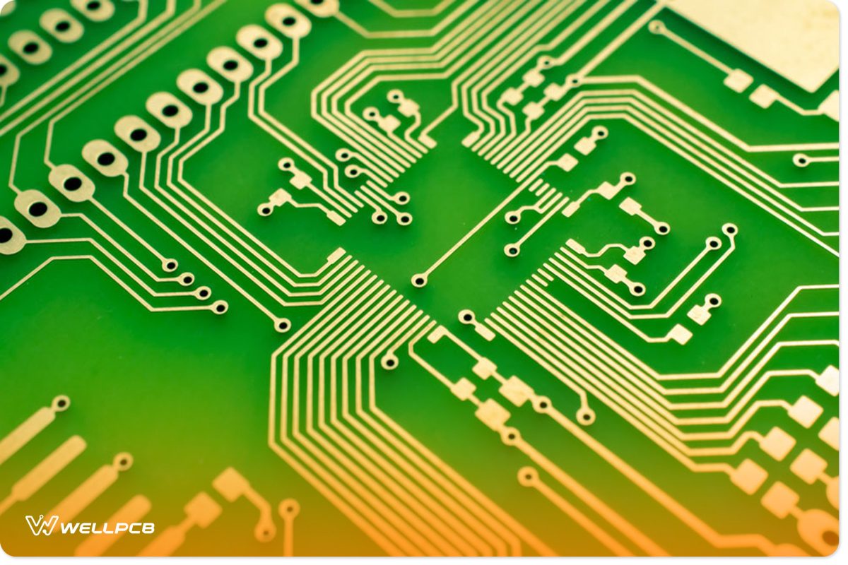
PCB Trace
The PCB trace is an essential aspect of any PCB design. It determines your circuit’s resistance and heat build-up.
In truth, you’ll start with a default trace width when designing a new PCB. However, this default trace width isn’t adequate for a high-current PCB. Hence, you’ll need to adjust your trace width according to its current carrying capacity.
High-current boards require more minor traces. These traces take up less board space and reduce your component cluster. On the other hand, trace thickness can range between 35 to 50 microns if your operating current is over ten amps.
Additionally, it’s normal to get inaccurate calculations on your first try. And it’s because many factors determine your trace width, including copper layer thickness, trace position, etc. Hence, it can be a complex process.
Luckily, you can make things easier with a PCB trace width calculator.
You Don’t Need Solder Masks
Solder masks can dampen the current capability of your traces. So, you’ll need to expose the underlying copper by removing your solder masks. No doubt, it would help increase your board’s current capacity.
But that’s not all. Removing solder masks means having extra solder. So, you can add them to the board’s trace to minimize resistance and increase thickness.
Also, you won’t have to increase trace width or spend on extra copper thickness. Instead, the solder will help increase current flow.
Copper Bars Work for Very High Currents
Copper bars save the day in applications where copper traces are not enough. Such applications include high-power inverters or other applications that generate current beyond 100A.
In truth, using copper traces in such circuits could cause severe meltdowns. However, copper bus bars are more durable for carrying currents and can handle heat. The best part is that you can solder these bars on PCB pads.
Isolate Heat-sensitive Components
Not all electrical components are tanky. Some are pretty sensitive to heat or changes in temperatures.
So, what can you do about such components? Simple, you can thermally isolate them. But unfortunately, high-current boards are all about heat, and these components wouldn’t be a great fit.
Also, thermal isolation includes adding board cutouts or using thermal relief connections for your boards.
Short Traces Work Best
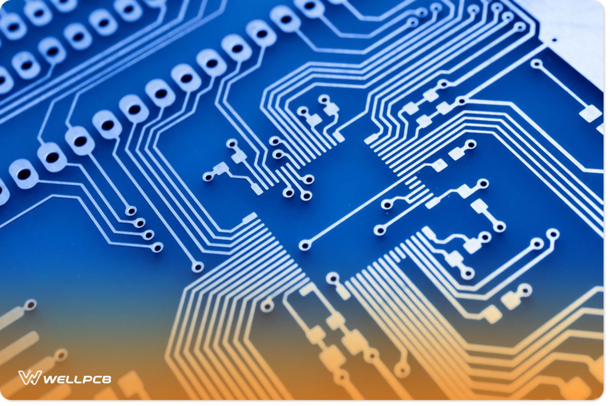
PCB Traces
But, the longer your traces, the higher your resistance. And the higher your resistance values, the more power you’ll lose.
Also, losing power generates a buttload of heat, which is not great for board life. Hence, it would help if you kept the traces for your high-current boards short.
Multiple Layers and Traces? Use Via Stitching
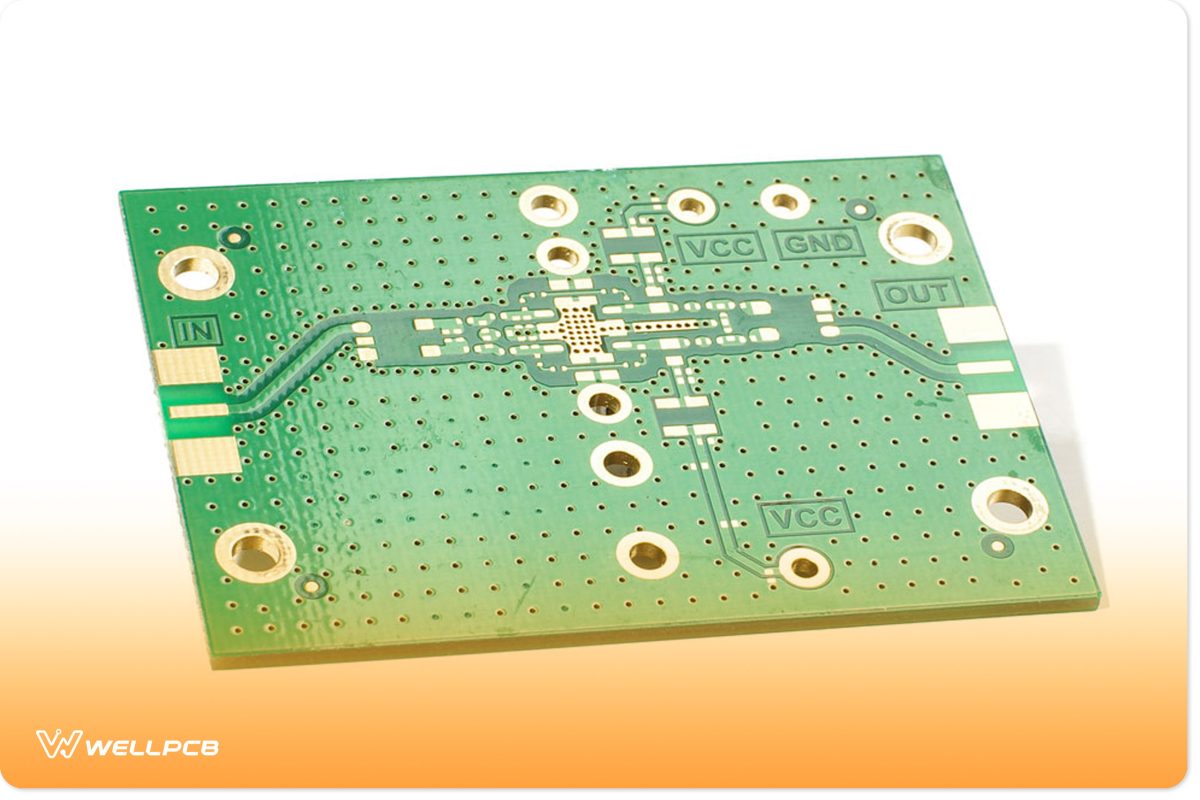
PCB Via
Sometimes, a trace might not be enough for the needed current. These situations happen when your board only has a single layer.
Interestingly, you can route your trace to multiple layers and increase the current capacity. Interestingly, you can use stitching to link your layers. However, ensure both layers have the same trace thickness.
Internal Layers can Create High Current Paths.
You can’t always have space for thick traces on your PCB’s outer layers. But you can have solid fills on your internal board layer in such a situation.
Don’t worry if you have high-current devices on your outer layers. Your vias can link them to your internal layers.
High-current components need Polygon Pours.
There are specific applications like processors and FPGAs that require high current flow. So, for these applications to work, you must activate high current flow in your PCB. But, in truth, you can do it with polygon pours.
Indeed, you can add square polygon pours beneath your chip and connect them with a visa. Then, link the polygon pour to your thick power traces.
Tips to Improve Your High-Current PCB’s Layout Effectiveness
Creating a successful high-current PCB design isn’t where the work ends. You’ll need to improve your PCB’s design and make them even more effective. Here are a few tips:
Tip 1: Right Angle Traces are not Effective
Avoid positioning your traces at right angles if you want an improved PCB design. Why? That’s because right-angle traces hinder trace uniformity.
Alternatively, you can position your traces at 45-degree angles. This way, your designs would look spacy and less clustered.
Tip 2: Pick your Line Width Carefully
It may not seem obvious, but line width is also essential. For this reason, you must select it carefully.
A suitable line width would smoothen the current flow, allowing your PCB to dish out a more effective performance.
Tip 3: Spacing is essential! Use it Adequately
Always space your components correctly. Do not create designs that cluster your parts. You’d be building a disaster.
Tip 4: Avoid using One Wiring Position between Layers
Remember to keep your wiring positions between your layers dynamic. The reason is simple. Various layers will need different directions. Thus, using different wiring positions would generate better results.
Tip 5: Feel Free to DIY!
The standard method isn’t always the best choice. Thus, you can always use some DIY to improve your PCB layout. After all, creating a grand schematic requires using all the tools at your disposal.
Benefits of High Current Heavy Copper PCBs
Heavy copper PCBs are excellent for high-current applications, and here’s why:
- Heavy copper PCBs have exceptional thermal resistance. Hence, they are more suitable for high-speed, high-frequency, and harsh temperature applications.
- Heavy copper PCBs are pretty durable with excellent mechanical strength.
- Thermal conductivity is also one of the benefits of heavy copper PCBs. These PCBs offer effective heat sink properties.
- You can also get heat dissipation features from heavy copper PCBs. They can help counter overheating and avoid damage.
- Electrical conductivity? Check! Heavy copper boards are excellent conductors that work well in electronics.
Final Thoughts
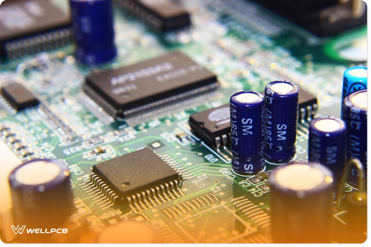
Printed circuit board with Components
In truth, you can’t build high-current applications without high-current PCBs. Standard PCBs can’t handle the heat and would end up burnt or destroyed.
However, these high-current boards possess the right features to handle applications that require high-current. They also have enough thermal durability to tank the heat generated from high currents.
So, do you want to build a high-current PCB? Be sure to contact us.


