Contents [hide]
What is a Printed Circuit Board?
A printed circuit board (PCB) is a collection of embedded wires running through a flat fragment of fiberglass. This rigid structure is used to mechanically support and electrically connect electronic components. It’s a crucial element in almost all modern electronic devices.
Printed circuit boards became widespread in the latter half of the 20th century. Before then, manufacturers connected an appliance’s components through point-to-point wiring, which was typically disorganized and messy. The creation of PCBs sought to solve this issue.
During the modern PCB fabrication process, the manufacturer stacks slices of fiberglass together and treats them with a chemical resin, which bonds them together.
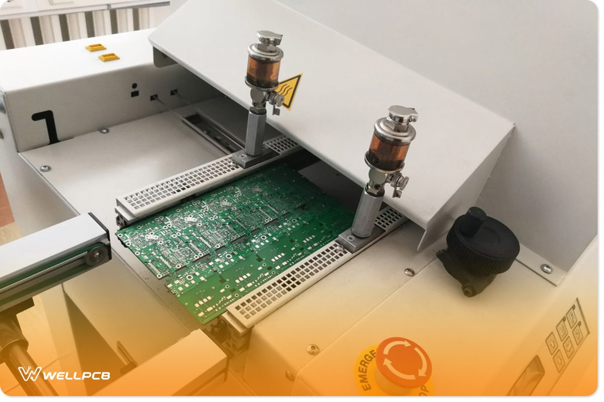
Printed circuit board after complete assembly moves to reflow oven machine
Next, the manufacturer applies a copper layer to both sides of the fiberglass slab. Then, they apply photoresist. After that, they etch a PCB layout pattern that matches the traces on the board. From there, they harden and dry the board with UV light.
With that done, the manufacturer washes the board with warm water, which cleans the uncovered areas, leaving the tracks of copper. These tracks serve as a base for how the PCB will look after the copper etching process.
Depending on the board’s specifications and design, the manufacturer drills mounting holes for connections and components.
In general, the PCB is just a collection of electrical connections on a substrate. So, you don’t necessarily need a fancy manufacturing process to make a simple circuit board at home.
Easy Ways To Fabricate a DIY PCB Board for Beginners
It’s possible to make your own simple circuit board. Whether you’re a hobbyist or a student, these beginner-friendly methods can help you create a functional PCB for your electronics projects.
Each technique comes with its own advantages. Choose the one that best fits your tools, budget and project requirements.
Use an iron and glossy paper: Also known as the toner transfer method, this strikes a balance between accessibility and precision. By transferring a printed design onto the copper board using heat, this technique achieves fine details with minimal effort, making it perfect for beginners.
Laser etching: A precision-based approach that leverages a laser engraver to remove unwanted copper, leaving clean, professional-grade circuit traces. This technique is ideal for intricate designs but requires access to specialized equipment.
Hand drawing the circuit design on the board: A more hands-on and budget-friendly option that involves sketching the layout directly onto the copper board using a marker or etching pen. It’s perfect for simple circuits and allows you to get a deeper understanding of the design process. However, it often lacks the accuracy of other methods.
How To Make a PCB at Home
Here, we’ll cover how to make your very own DIY PCB. Because the toner method is both beginner-friendly and easy to access, we’ll focus on giving you instructions for this method.
One of the essential components you require to get started is PCB design software. Luckily, there is a host of great open-source design software to help you create your circuit designs. They include:
- Autodesk Eagle: Read tutorials
- KiCad: Read tutorials
- Fritzing: Read tutorials
- DesignSpark PCB: Read tutorials
- ExpressPCB: Read tutorials
- PCBWizard: Read tutorials
Each of these tools has tutorials and documentation to help you learn how to design PCB layouts. Once you have created and printed your desired design based on PCB layout guidelines, you can proceed.
Besides PCB design software, circuit simulator tools like LTSpice, Proteus, or Multisim are incredibly useful for testing your circuit virtually before bringing it to life.

Required Tools and Materials for a Homemade PCB
Here’s a complete list of the materials you need to fabricate your PCB using the toner transfer method.
- Old magazine paper or advertising brochures with glossy print
- Old newspaper
- Laser or inkjet printer
- Clothes iron
- Copper-clad laminate sheet
- Ferric chloride powder solution (FeCl₃ etching solution)
- Dish wash scrubs/steel wool
- Acetone (nail polish remover/thinners)
- Rubber gloves
- Plastic box/plastic container
- Teaspoon
- PVC wire
- A4 photo/glossy paper
- Sandpaper
- Black permanent marker
- Blade cutter
- Sandpaper
- A roll of paper towels
- Cotton wool
- Clear tape
- Brown paper
- Oven mitts
Step-by-Step Instructions
In this tutorial, we’ll guide you through creating a simple PCB that connects to a 555-timer chip. This will allow you to build or integrate a touch switch into your project. ore proceeding with the instructions in this section, please ensure you have all the materials and tools.
Step 1
Print your PCB layout design using an inkjet or laser printer. Set it to print in black/grayscale. You can configure the settings on the PCB design software and the printer driver settings.
For the purposes of fabricating a PCB, ensure that it’s a mirror printout and print on the glossy side of the photo paper. Once it’s printed, cut out the design.

Step 2
Cut a square piece from the copper-clad laminate using a blade cutter. When cutting, use the printed PCB layout as a size reference.
Step 3
Use steel wool or a kitchen scrub to rub the copper side of the cut-out laminate, removing the top oxide and photoresist layer. This makes it easier for you to stick the PCB layout design on the copper.
Step 4
Transfer the printed PCB layout onto the top of the treated copper laminate layer (which will serve as the final PCB). Ensure the glossy portion of the paper is facing down and aligned with the side of the copper laminate.
Step 5
Next, place the brown paper on top of the copper piece and the printed design paper. Press and iron the design onto the copper piece, with the brown paper serving as protection. While doing this, you need to ensure:
- You are using a flat wooden or granite surface
- The iron is not set to steam
- Iron slowly while applying steady pressure
- The copper board is secure – you can use a pair of pliers

Image of clothes steams iron. Warm the clothes and iron them until they reach their maximum temperature.
If you do it properly, the entire transfer process should take up to 10 minutes. However, if you’re not comfortable using an iron, you can transfer the design onto the copper face using a pencil and a permanent black marker, although it’s not as effective.
Step 6
Use oven mitts to transfer the copper piece into a bowl, sink, or container of lukewarm water. Leave it in the water for 10 minutes. Finally, gently separate the paper from the copper. The most effective way to do this is by peeling the paper from the copper at a low angle.
Sometimes, the design may not wholly show up on the copper face. In that case, you’ll need to use your permanent black marker to fill out any missing lines.
Step 7
Next, it’s time to etch the plate. Put on a pair of rubber gloves and cover your floor, desk, and counter with brown paper or newspaper. Accordingly, this will prevent the etching solution from spoiling them.
Fill up a plastic container or box with water and place three teaspoons of ferric chloride powder into it. Carefully stir until you dissolve the solution. Next, dip the PCB (a copper piece) into the solution for thirty minutes or until the process unmasks the copper.
Use pliers to check if the etching process is complete. It should remove any unwanted copper from the final product.
Be careful when using the ferric solution – it stains surfaces and is corrosive. Using a plastic container and performing this step in a well-ventilated area is crucial.
Step 8
Once you have etched the PCB, dilute the rest of the ferric chloride solution and carefully store it for disposal. Do not pour it down a drain or flush it down the toilet. Because it’s a hazardous material, it could damage your plumbing and pipes. It’s best to contact a hazardous chemical collection service in your town and get them to dispose of it.
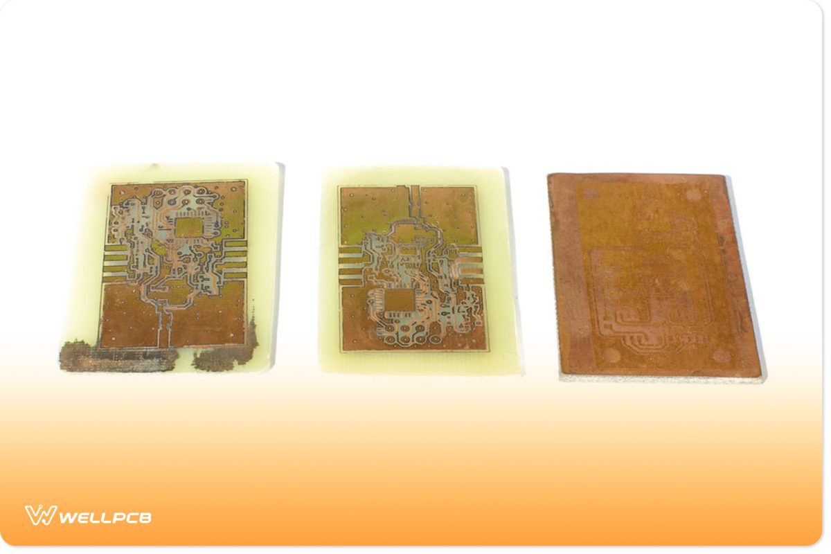
Use a few drops of acetone (nail polish remover) on a piece of cotton wool to wipe away the ink/toner on the PCB to reveal the copper layout. Next, clean and rinse the PCB with warm water and dry it with a paper towel.
Finally, use sandpaper to trim and smooth the edges of the PCB. You can create through holes with a micro-electric drill. Alternatively, you can solder your electronic components directly on the PCB. For a more traditional look, paint it with green or red UV-curable solder paint.
Once that’s done, clean up your work area, and you have yourself a solid homemade PCB.
Fun DIY PCB Projects
There are so many fun and affordable PCB projects you can create. And they only require basic know-how to get everything going. Here are a few that may find their way into your everyday life!
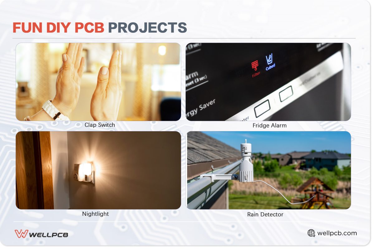
Clap Switch
Everyone can use a handy clapping switch for their lights and other gadgets at home. When you clap, the circuit picks up the sound and turns your connected electronics on or off.
Fridge Alarm
This one is perfect if you or anyone else leaves the fridge door open for a long time. It blares out a beeping alarm in that scenario, alerting someone to close it.
Nightlight
You can create a nightlight PCB to help you see and move around at night. It uses common components, like an LDR and 555 IC, that detects darkness and brightens up the room.
Rain Detector
These simple circuits inform you when it starts raining. They use an Attiny85 IC and rain sensor module to detect raindrops.
Conclusion
Creating a DIY PCB board can be a rewarding experience for beginners. Going through the motions gives you a deeper understanding of electronics and the satisfaction of building something functional from scratch.
However, while homemade PCBs are great for hobbyists and beginners, they can’t match the precision, quality, and durability of professionally manufactured PCBs.
When your projects demand more advanced capabilities, WellPCB is here to help. As an experienced manufacturer, WellPCB takes the complexity out of PCB fabrication, delivering expertly crafted boards tailored to your specifications. Our expert team provides a seamless and stress-free experience, making us the trusted choice for all your PCB needs.
Common FAQs
Can Anyone Easily Make a PCB?
In theory, anyone can make a printed circuit board. It’s both hard and easy to make, depending on the project. The more components you have to handle, the more complicated things get. It’s always a good idea to use turnkey PCB assembly services to ensure you get the most value and efficiency for your projects.
Is It Possible to 3D Print a Printed Circuit Board?
Yes, a 3D printer can fabricate PCBs. For this to work, you may need to use aerosol jet printing to get the traces onto the board.
How Do You Tell If Your PCB Is Faulty?
The best way to tell if there are any issues with your PCB is to take a close look at your circuit board and components. If you see any cracks, chips, corrosion, or burns, you might experience functionality issues with the board.