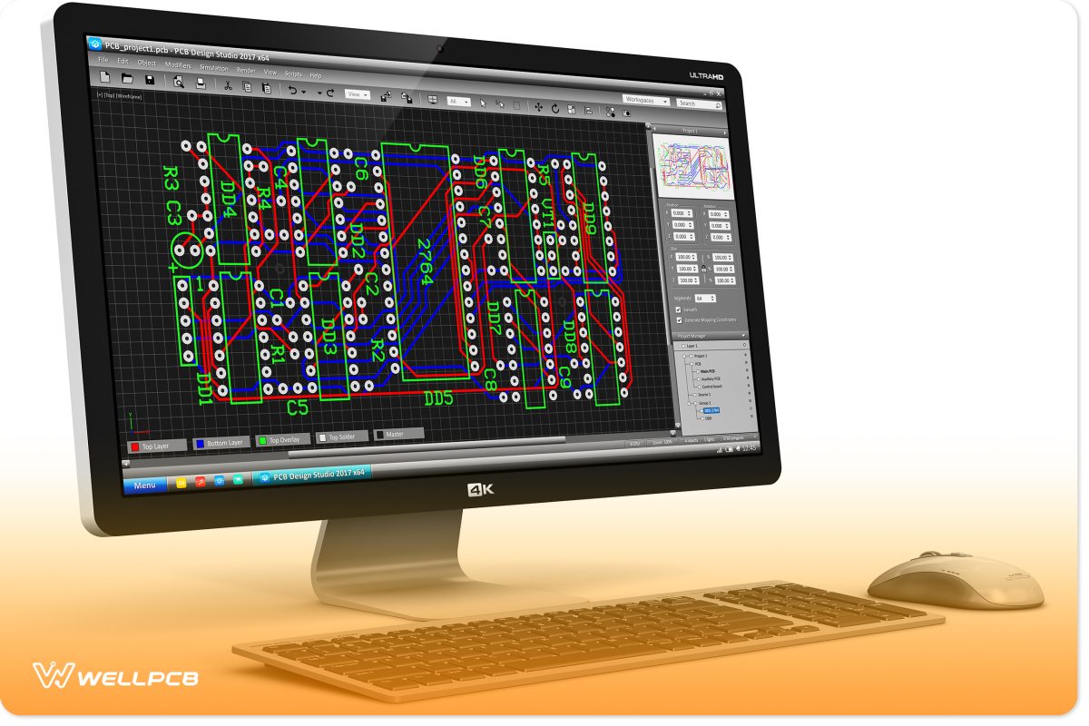
Custom pcb design-Transfer
Take the printed paper and cut it to the size of the PCB.
Place this paper on the copper layer facing the printed area towards the copper surface.
Use the document laminator, and Preheat it now; pass the copper PCB and paper carefully through the laminator. Do not let them move while passing through the laminator. Carefully repeat this 2 to 3 times until the paper completely sticks on PCB. Now let the PCB cool down. If you don’t have a Laminator, then you can use electric iron. Heat the iron to its maximum setting; once it’s hot, carefully place the paper on the PCB, same as for the laminator, and rub the hot iron on the white, nonprinted side of the paper. And rub it till the paper is completely stuck to the PCB.

It will take 10 to 20 minutes to stick completely stick the paper on PCB let the paper turn slightly Brown now you are ready to take the paper out. Let the PCB cool down to normal temperature room temperature. Do not add water to cool. Once the PCB is cooled, carefully try to remove the paper from the PCB surface. You will see all the black ink from the paper is now on the copper surface, and the remaining paper will come out, so now you have your PCB layout on the copper surface.
Carefully check the PCB layout for any cracks or misspouts. If you find any cracks or misprints, repair them with any oil-based paint. The best way is to use high-quality permanent marker pens. Once you confirm that the layout, is ok, you are ready for the next stages.
Custom PCB Design-Etching
For etching, you have to purchase Chemicals like ferric chloride or sodium persulphate from your local chemical store.

You can use any plastic container for this process. Dip the PCB in the container with the etching solution and let the exposed copper dissolve in the chemical. It will take about half an hour to dissolve the remaining copper in your etching solution completely. Keep checking from time to time until you see a finished PCB. Unnecessary copper is removed. Please take out the PCB, clean it with normal tap water, and then use a kitchen scrubber to remove black ink from the copper surfaces. Now, you will see a fully finished PCB. Now you can go for drilling and mounting components.


