Contents
1 . Conversion and technology
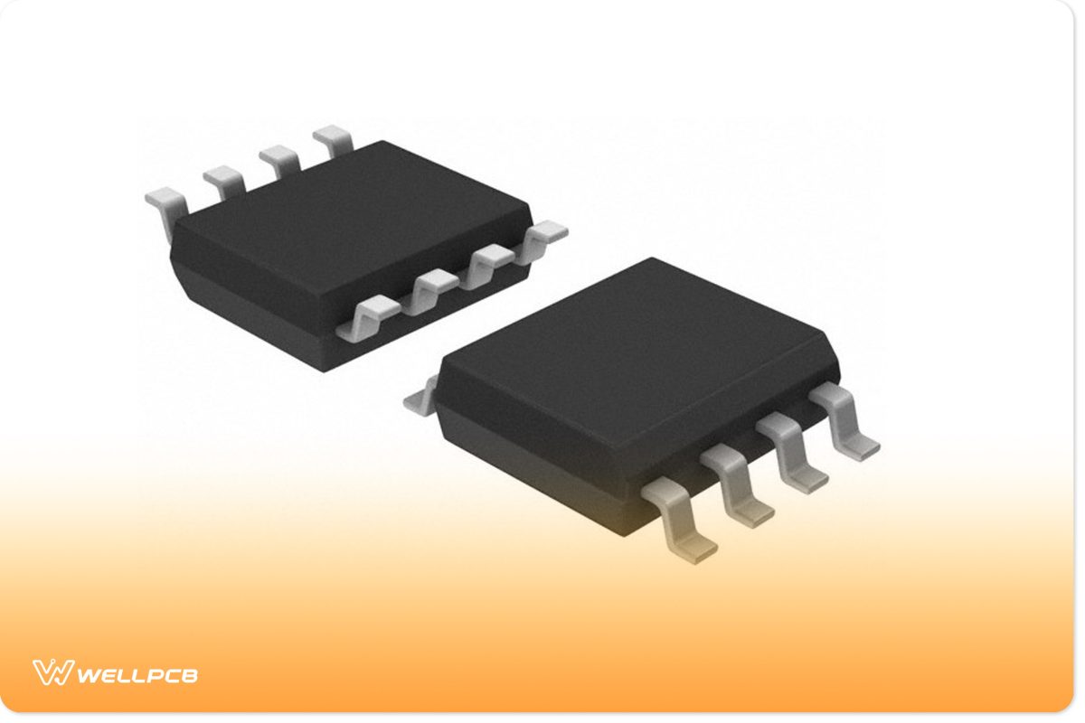
The small outline integrated circuit(SOIC) usually takes only 30- 45 % of the total space required by their dual in-line package counterparts.
Small shape integrated circuits only have 30 % thickness of the DIP package. Small outline integrated circuits have an identical pinout.
And the performance other than the surface area.
Some of them are made to consume less power than the equivalent DIP package in some cases. For low power applications of that particular package.
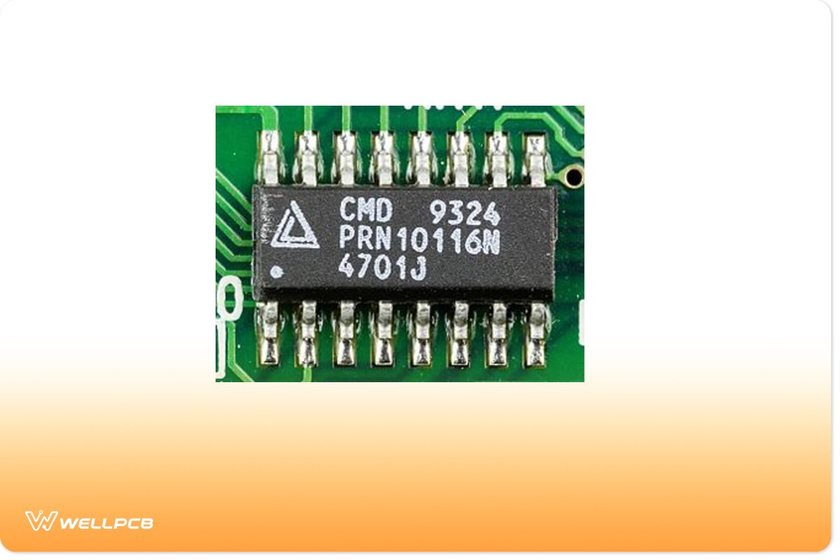
The part numbers on the packages are sometimes shortened to fit in the reduced area. SOIC has been widely used since the late ’70s.
The small outline integrated circuit has package information stated with the prefix SO.
The number following the prefix is usually the pin count of that specific integrated circuit.

2. SOIC standards and types
Integrated circuit packaging is regulated and standardized to optimize the installment.
And to reduce the machining cost during the proception of printed circuit boards and integrated circuit systems.
The package and pin sizes are made concerning a small outline integrated circuit.
Which are from the Electronics Industries Association of Japan and JEDEC solid-state technology association standards.
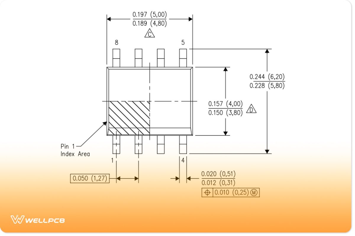
Although the EIAJ model had a body diameter of approximately 5.3 mm, the diameter depends entirely on the device.
Since there are many variants with different structural measurements, but, in most cases, small outline integrated circuits have a lead spacing of 1.25 mm.
SOIC has several variants, such as the small outline J-leaded package(SOJ), the shrink small outline package(SSOP), the small mini outline package(MSOP), and the small thin outline integrated circuit package(TSOP).

Each variant has a different body size and thickness, but they all have the exact pin mapping and circuit configurations.

3. Advantages of Small outline integrated circuit
The significant advantage of small-outline integrated circuits is the footprint reduction.
This reduction in space consumption results in smaller printed board sizes.
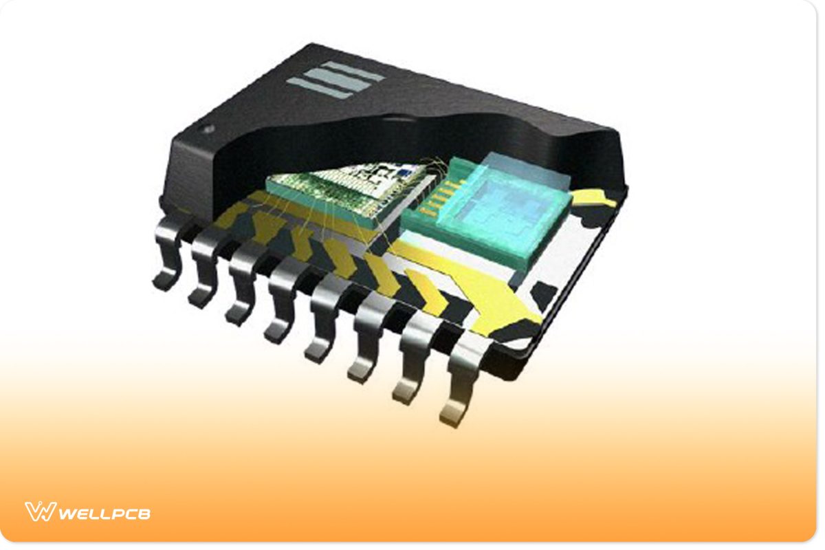
SOIC also reduced the fabrication cost of the integrated circuits by reducing the materials used in the packaging.
Smaller size components are accessible to the pcb assembly by a machine than a more significant size package. Since small outline integrated circuits are practically SMD, multi-layer boards are only possible through these types of packaging.


