Contents
- 1 What is Conformal Coating in PCB Manufacturing?
- 2 Benefits of Using Conformal Coating on PCBs
- 3 Types of Conformal Coating
- 4 How Is a Conformal Coating Applied to a PCB?
- 5 Choosing the Right Conformal Coating for Your Needs
- 6 Are There Any Drawbacks to Using Conformal Coatings?
- 7 Choose the Right Conformal Coating for your Next Project
What is Conformal Coating in PCB Manufacturing?
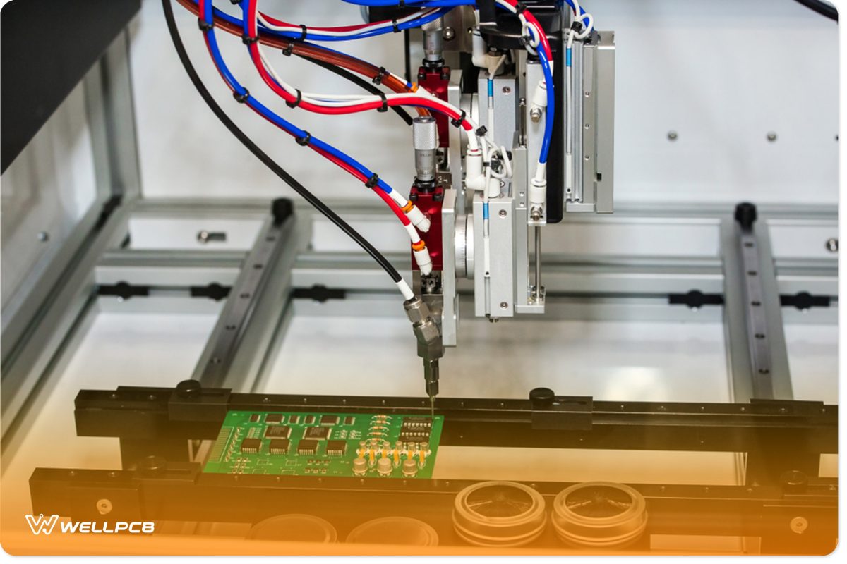
[Image: Robotic system spraying conformal coating. ]
Conformal coating is a thin polymer layer applied to the surface of a printed circuit board (PCB).
This coating protects the PCB and its integrated components against harmful environmental conditions, such as moisture, dirt, humidity, chemicals, salt spray, and extreme temperatures.
When applied, the coating adheres to the shape of the PCB and all its components. It covers traces, component leads, solder joints, and metallicized parts, providing a protective barrier that helps prevent corrosion.
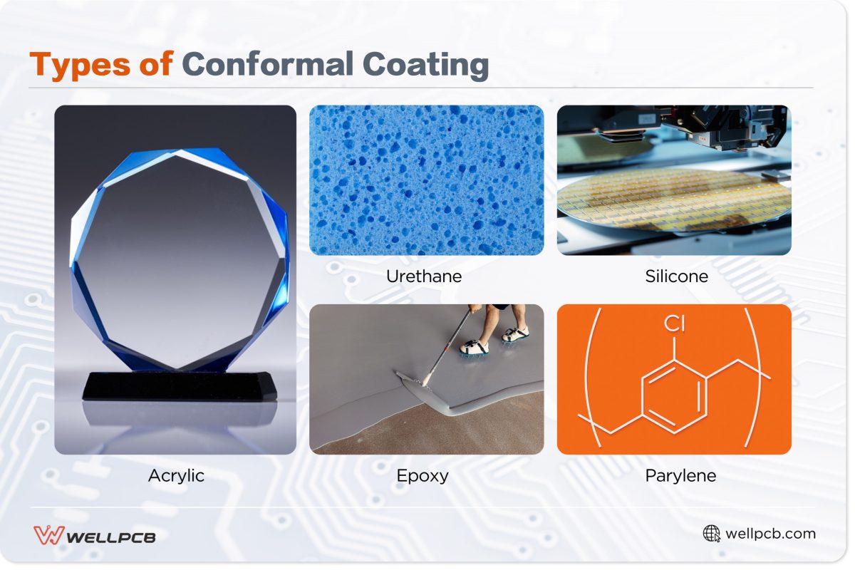
Common types of conformal coating include acrylic, urethane, silicone, epoxy, and perylene.
Benefits of Using Conformal Coating on PCBs
Conformal coating is widely used across industries because its advantages significantly outweigh potential drawbacks. The key benefits of using conformal coating on PCBs include:
- Corrosion protection
The thin conformal coating layer acts like a shield by sealing the PCB surface away from humidity and moisture, which helps prevent corrosion.
- Improved electrical performance
The coating provides insulation to the PCB components, reducing crosstalk and leakage. This means electrical paths won’t interfere with each other or impact nearby circuits.
- Resistance to thermal stress, vibration, and shock
Conformal coatings help manage the effects of temperature changes, which may otherwise cause electrical components to expand or contract. Hotspots and thermal stress are less common as the coating spreads heat more evenly and acts as a thermal stabilizer. It also helps absorb any shock or vibrations the PCB may encounter, helping to keep all components in good condition.
- Protection from dirt, dust, and other contaminants
The protective layer keeps dirt, dust, and other harmful materials away from important PCB parts, like solder joints, connections, and integrated circuits (ICs). This prevents interference and keeps the PCB working as intended.
- PCB components last longer
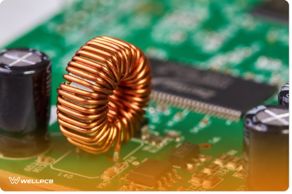
[Image: Close-up of components.]
With conformal coating, PCB components work reliably for longer, as dust, chemicals, harsh temperatures, and more won’t affect their lifespan. This significantly reduces the risk of eventual damage or failure.
Types of Conformal Coating
[Image: Types of Conformal Coating.]
Different types of conformal coating are used in PCB manufacturing, each with unique properties that strengthen a circuit board. These are some of the most common coating materials.
Acrylic
Acrylic coatings are easy to apply and remove, are inexpensive, and cure quickly at room temperature thanks to solvent evaporation. They are also transparent enough for components to be seen clearly throughout their use without the risk of darkening.
However, an acrylic conformal coating provides little to no protection against solvents and chemicals. This coating type is used in aerospace, automotive, electronics, and medical devices.
Pros:
- Clear
- Quick curing
- Easy application and removal
Cons:
- Not very resistant to chemicals
Urethane
Urethane conformal coatings are highly durable and can handle mechanical stress, high-voltage arcing, and abrasion. As such, this coating is effective at extending the lifespan of devices.
Urethane is also flexible and bends without peeling or cracking. Additionally, this coating resists chemicals, like corrosive agents and solvents, that could cause failure, making it ideal for use in industrial environments.
Pros:
- Rigorous
- Flexible
- Moisture and chemical-resistant
Cons:
- Prone to yellowing
- Difficult to rework or repair
Silicone
Silicone coatings have low thermal conductivity and can withstand extremely high temperatures—up to 400°F. This makes them ideal for protecting PCBs with heat-producing components.
Silicone is also hydrophobic with a low water vapor transmission rate (WVTR), keeping moisture off the circuit board. Silicone works best in high-temperature environments, as well as aerospace.
Pros:
- Flexible
- Guards against moisture and extreme temperatures
Cons:
- Costly
- Tough to remove
Epoxy
An epoxy conformal coating is highly resistant to chemicals, like solvents, making it ideal for extreme industrial environments. And as epoxies have two compounds combined into one layer, they are especially tough and durable. This makes them effective at protecting against mechanical stress and abrasion.
Pros:
- Chemical resistant
- Protects against mechanical stress and abrasion
Cons:
- Difficult to rework
Parylene
A perylene coating is ultra-thin and evenly spread across a circuit board’s surface via vapor deposition. Parylene can protect PCBs from mechanical and thermal stress, chemicals, dirt and dust, and humidity without additional materials. It also conforms to the unique shapes of components and PCBs.
Since perylene is biocompatible, it’s suitable for medical device and implant applications. This coating is safe for patients both inside and outside the body, so it’s used in cochlear implants, pacemakers, and more.
Pros:
- Prevents moisture and chemical penetration
- Extremely thin
Cons
- Very expensive
- Difficult to apply on a PCB
How Is a Conformal Coating Applied to a PCB?
PCB manufacturers follow a multi-step process when applying a conformal coating. In this section, we’ll explore this process in detail.
Cleaning
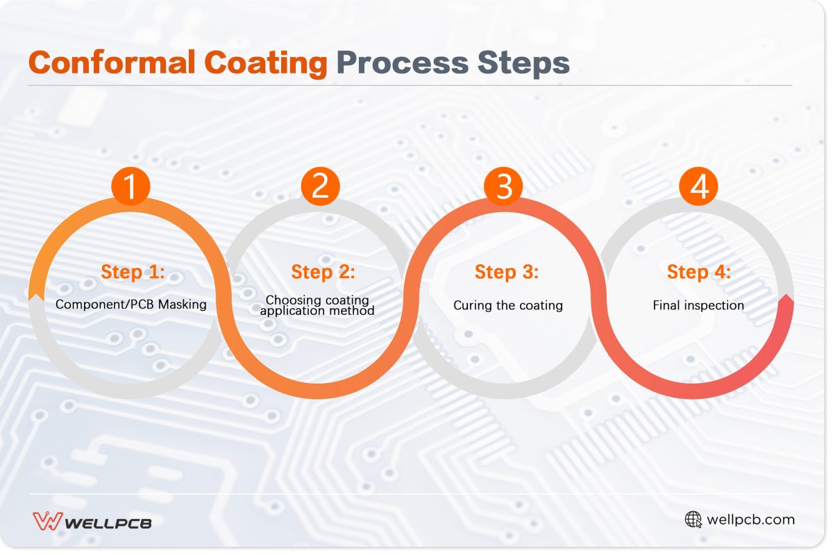
Before applying a conformal coating, the PCB must be free from contaminants such as flux, oil, and grease. Contaminants can lead to defects, including component failure, de-wetting, corrosion, uneven coating coverage, and bubbling.
Cleaning products like PCB cleaning sprays, flux removers, isopropyl alcohol, ultrasonic cleaners, and deionized water are essential for this step.
Component/PCB Masking
Masking takes place next. A peelable solder mask or painter’s tape is applied to components or contact points that do not need coating. This ensures these parts aren’t damaged during the coating process and that the coating doesn’t disrupt electrical performance.
Application Methods
There are three different conformal coating application techniques.
- Spraying
Typically, a pneumatic spray gun is used to apply the coating. Operators often prefer this method for better edge-tip coating of a PCB, quicker turnaround, film uniformity, and high-volume production.
The spraying method may involve an automated selective coating machine to achieve high-precision spray thickness and patterns on a high volume of PCBs.
Alternatively, an operator might use a spray gun in a spray booth. In this case, they position the spray gun at a certain distance from the PCB surface and overlap multiple strokes.
- Dipping
The circuit board is dipped in conformal coating, creating a protective layer. Although this method can be messy, it works best for low-volume PCBs. Components that don’t require coating need masking beforehand.
The PCB is fully submerged in the coating solution to achieve an even layer. The thickness is usually controlled by adjusting the dip and withdraw speed.
- Brushing
A brush is used to apply the coating to the PCB. While this method is ideal for repairing and reworking worn-out coatings, it takes longer to finish than the others.
The coating must first be applied to the bristle to cover the surface with a brush evenly. Brushing is done with smooth and consistent strokes to ensure an even layer.
Cure
There are three methods to cure the coating: UV, thermal, and moisture.
- UV cure: This method is used for acrylic, silicone, and methacrylate coatings. It involves exposing the coating to high UV for a quick drying process.
- Thermal cure: Heat is suitable for polyurethane, acrylic, and epoxy coatings. It also cures solvent-type coatings through solvent evaporation.
- Moisture cure: Ideal for silicone and polyurethane coatings, this method relies on airborne moisture to cure the coating. As such, the curing process goes faster in higher humidity.
Final Inspection and Testing
[Image: Inspecting the PCB. ]
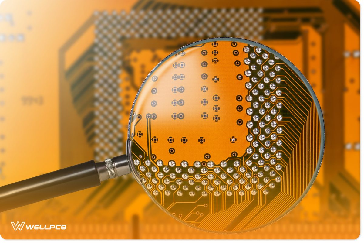
The final step is to inspect the PCB to ensure proper conformal coating coverage and functionality.
Placing the PCB under a UV light, like a black lamp, will reveal a blue light that indicates the correct coating application.
Any circuit board parts without fluorescent light represent incorrect coating coverage or defects.
Electrical testing determines whether the PCB will work, regardless of the applied coating.
Insulation resistance measurement, impedance testing, and continuity testing can help identify issues, including short circuits.
Another way to test PCB functionality is to expose it to chemicals, humidity, salt spray, and harsh temperatures.
This demonstrates how well the coating protects against environmental hazards.
Mechanical stress testing, like abrasion and bending tests, ensures the strength and durability of the adhesion and coating.
Doing so will verify that the coating will stay in place and won’t break under mechanical stress.
Choosing the Right Conformal Coating for Your Needs
Conformal coatings vary, so the right coating for your needs will depend on your PCB use case. Here are some considerations to consider when deciding on a suitable coating material.
Environmental conditions: Consider factors like temperature and humidity. Certain coatings withstand high temperatures, while others may become brittle and break easily. Similarly, conformal coatings with moisture-resistance qualities will keep your PCB safe in extremely humid conditions.
Required level of protection: Flexible coating materials like urethane and silicone are an ideal choice for PCBs exposed to regular mechanical stress, like shock or vibration. Epoxy and urethane coatings, on the other hand, have the best chemical resistance — making them ideal for protection against chemical exposure. If your PCB will be used in areas with high moisture, parylene and silicone are a good option. Parylene is also excellent for electrical insulation.
Compatibility: Always make sure the coating material is compatible with your PCB. This ensures the components and circuit board won’t sustain damage over time.
Coating properties: If you need to inspect PCB components, a clear coating, like perylene or acrylic, is suitable. For this purpose, PCBs that bend will need a flexible coating, making silicone or urethane the preferred coating type.
Costs: Consider the costs associated with conformal coating. The application technique and materials used, for instance, all contribute to total expenditure. Perylene is particularly expensive because it relies on vapor deposition and uses dimer raw materials.
Contact us for a free consultation to learn more about how our conformal coating solutions can protect your electronics.
Are There Any Drawbacks to Using Conformal Coatings?
Nevertheless, conformal coating has some downsides that can affect the PCB’s cost and function.
Increased Processing Time and Cost
End customers will face higher costs and longer processing time for coated PCBs than uncoated PCBs. The job requires special equipment and tools, additional materials, and a more complex assembly process.
Improper Application
Applying the coating incorrectly may cause deformities, such as fish eyes, orange peel, bubbling, de-wetting, and overspray.
These can all cause performance degradation by weakening the coating, leading to greater mechanical or environmental stress vulnerability.
Due to the lack of insulation from the bubbling or fish eyes, components may also short-circuit, crosstalk, or undergo electrical leakage.
Component Rework or Repair
Due to the coating’s strong adhesion, fixing components under it can be challenging.
Cutting away or removing the coating to gain access to components can damage certain parts unless special equipment is used.
The coating’s mechanical strength and solvent or chemical resistance also tend to make repair attempts more difficult.
Choose the Right Conformal Coating for your Next Project
Conformal coatings enhance the strength and durability of a PCB by providing a protective barrier against potentially damaging environmental hazards. They also improve electrical performance, making the device more reliable.
Importantly, conformal coatings prevent PCB components from degrading or failing quickly — which is vital for electronic device manufacturers across industries.
Contact us today to discuss your conformal coating needs. Use our free online tool to get a quote for your next PCB assembly project.


