BGA Assembly
- BGA, abbreviated as ball grid array, is an SMT package type made for integrated circuits.
- BGAs have more interconnection pins than regular chip carriers—placed on a flat package or dual in-line.
- All BGA devices adopt specific soldering control. And automated processes are responsible.
- Professional engineer review; strict quality control for each process.
- Advanced Testing Technology To Ensure the Quality such as AOI Test, E-Test, X-RAY, Impedance Control.
- We committed to helping customers get the highest quality products and services with competitive prices (especially multilayers PCBs).
- FR4,High TG FR4, High-frequency Material, Rogers PCB, Metal based PCB.
- Superior customer service (personal to personal).
Definition of BGA
BGA, abbreviated as ball grid array, is an SMT package type made for integrated circuits. They also create a lasting mounting for devices like microprocessors.
BGAs have more interconnection pins than regular chip carriers—placed on a flat package or dual in-line. The entire base surface of BGAs is useful, unlike other devices that only use their perimeter.
All BGA devices adopt specific soldering control. And automated processes are responsible. Hence, you’ll find this process in tech-controlled automated reflow ovens.
Types of BGAs
Every PCB manufacturer has the specific adopted BGA—used for different countries. But, the six BGAs below are by far the most popular types in the market.
Micro BGA
- Tessera first invented the micro BGA. This BGA has its chips facing down, while its substrates come from packaging tapes.
- Micro BGA is small, which makes them ideal for small high-tech products. Also, its pins are few, and it's the main component of high storage devices. Therefore, it has a lower liability and higher accessibility.
The package on Package BGA
- The POP ball grid array is a double-stack design—with the upper chip for RAM and base chip serving as the CPU.
- This type of BGA is ideal for a large number of packages fitting into small footprints on a PCB.
Plastic BGA
- Motorola invented the plastic ball grid array. Hence, it has the widest applications. JEDEC Level-3 verified the reliability of the plastic ball grid array. And it’s because it has a resin (bismaleimide triazine) merged with sealant technologies’ application or glob to pad array carrier.
- The plastic BGA’s sturdiness makes it the most used by a lot of PCB manufacturers.
Tape BGA
- The TBGA or tape ball grid array has sturdy core materials ideal for electrical connectivity and heat dissipation, especially for thin devices.
- The only snag is that it’s pricey. Hence, it’s more expensive than a plastic ball grid array.
Molded Array Process BGA
- Also known as MAPBGA, it’s a BGA type that uses its solder ball grid for electrical connections. On a substrate strip, you’ll see the different units arranged in a matrix array—singulated and merged by sawing.
- Also, mold compounds differentiate the singulated units of this BGA.
Thermally Enhanced Plastic BGA
- This type of BGA is mainly for enhanced SMT capacity, improved thermal processes, and low inductance devices.
- Furthermore, this BGA package uses semiconductor grade materials, making it sturdy for long-term processes and flexible design constraints.
The Merits and Demerits of BGA
Pros
- A BGA is more compact to use lesser space on a circuit board
- Heat dispels rapidly from a BGA because of its less thermal resistant feature
- It has a high conductivity level
- The BGA is self-aligning
The Applications of BGA
▶ applications
▶ Consumer Electronics
▶ Automotive Sector
▶ Flat Electronics Systems
▶ Integrated Circuits in TVs, computers, smartphones, etc.
How the BGA Assembly Works
BGA Reballing
- This process involves changing all the old soldered balls on a grid array assembly to new balls. Engineers employ this process on PC motherboards, gaming consoles, or laptops that have issues with their VGA cards.
BGA Soldering
- Manufacturers engage in BGA soldering by applying the solder reflow process with the help of a reflow oven. The BGA solder balls melt into the reflow oven during the BGA soldering process.
BGA Rework
- The BGA rework process involves an electronic component getting heated in a dedicated BGA rework station. And it has a vacuum device that boosts the package. It also has an infrared burner and a thermocouple that checks the temperature.
- Prototype orders placed within 24 hours
- Normal lead time (5-7 Wokring days for some PCBs prototypes and small batch production)
- Faster lead time (48 hours for some PCBs prototypes and small batch production)
The Method of Testing the BGA
Assembly Board
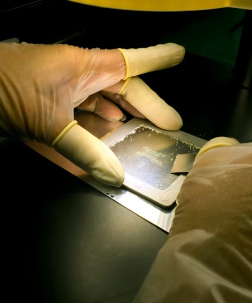
Testing a BGA assembly board involves searching for a soldering fault. And it isn’t easy to achieve this without using specific equipment. Also, the process helps to ensure that your PCB performs well.
Some of the tools you can use include endoscopes, industrial CT scanning machines, X-ray machines, JTAG, etc.
How do these tools help?
They have a 2D and 3D vision, which helps you to detect problems easily. You can spot things like solder thieving, solder balls, missing solder balls, excess solder, paste bridging, etc.
Testing also helps you to confirm the correct placement of the solder balls. Plus, it ensures there’s no issue with each contact pad.
With that said, using X-ray images has its snags. For instance, it may be difficult to spot parts in the same location. Or you may even notice interference with the X-ray with background metals like POP parts.
Hence, it would help if you had caution when you align the BGA with the board. Furthermore, the testing tools help to supplement precise placement and offer a measure of quality assurance.
Inspection of BGA Assembly with X-Ray
Like we mentioned earlier, X-ray machines are effective tools that show different defects. And the faults may show up during the BGA assembly. In summary, the X-ray solves soldering problems.
We have an X-ray support software, which helps to calculate the solder ball’s gap size. Also, it ensures that the BGA assembly follows IPC standards (Class III or Class II)—depending on your specifications.
But that’s not all.
Our skilled technicians use 2d X-rays. Hence, it makes it easy to provide 3D images that confirm problems like cold solder joints in BGA balls, via in pad BGA designs, and inner layers with buried or blind vias.
Capabilities of BGA Assembly
Our BGA assembly has automated placement systems (four). And they have Vision Systems that help to examine solder ball coverage.
An automated system with a 3D laser is also available. It helps inspect the automatic placement of the solder ball height of MBGA, CBGA, and PBGA. Plus, we confirm our BGA assemblies with a real-time X-ray system.
You can place your orders with a minimum size of 0.3mm. The minimum space between two BGA is 0.2mm. And the minimum distance to the circuit line is 0.2mm.
What if your specifications are higher?
Not to worry. All you need to do is state your specific requirements and leave the rest to us.
Why Are We The Leading BGA Manufacturer
in China?
One thing you can always count on is our vast experience in handling different types of BGAs. So, it doesn’t matter if you prefer complex components like DSBGA—we have got you covered.
In other words, you can trust us to produce high yield and high-quality BGA boards. Above all, we have state-of-the-art BGA placement equipment.
Plus, we offer highly customizable complete PCB assembly solutions and high-precision BGA assembly processes.
Get in touch with us today to get a free online quote.
Certification



Products Show
