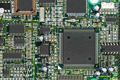
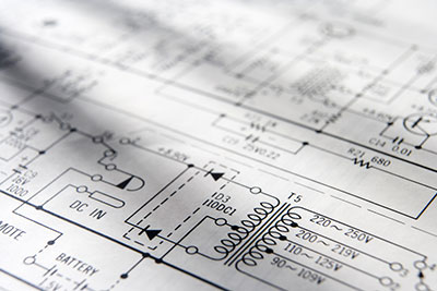
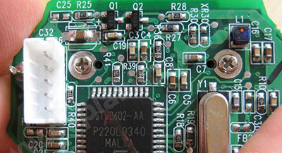
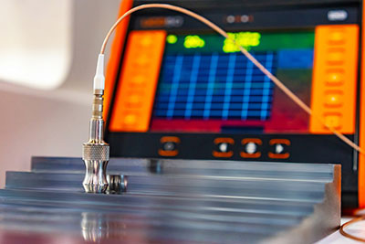
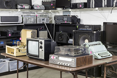
Blog
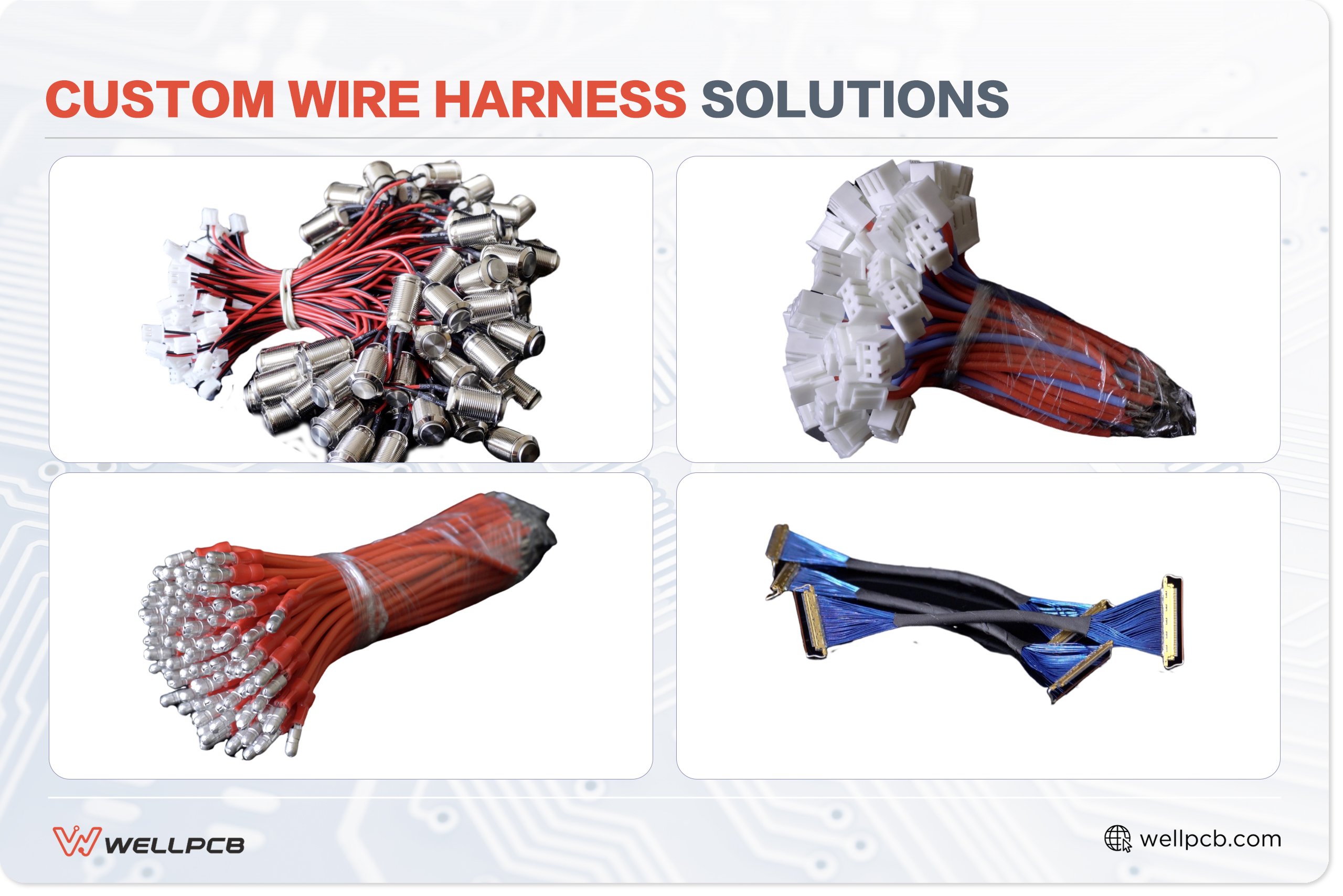
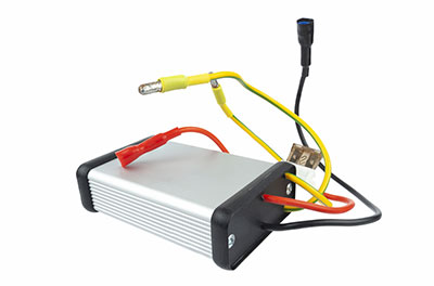
Elevating Your Products with Custom Wire Harness Solutions

Comprehensive Guide to Custom Wiring Harness

Top 10 Cable Manufacturers in the World

High-Performance Materials for Wiring Harnesses

Understanding Wiring Harness Components: Comprehensive Guide by WellPCB

Comprehensive Guide to Designing Electrical Wire Harnesses

Benefits of Custom Cable Assemblies in Manufacturing

Best Practices for Wire Harness Assembly in Aerospace Applications

How to Reduce Costs and Increase Efficiency with 3D Printing

Case Studies: How Businesses Are Using 3D Printing to Innovate

3D Printing for Custom Enclosures in Electronics: Enhancing Product Design and Functionality

Top 10 Industries Transforming with 3D Printing Technology

PCBs Fundamentals For Beginners! Collect Now!

12 Benefits of Turnkey PCB Assembly Services for Entrepreneurs

The Ultimate Guide to 3D Printing Services for Large Enterprises and SMEs

Circuit Simulators: A Guide to the Top 13 Tools

RJ45 Connector: Complete Pinout Guide and Applications (2024)

FDM vs. SLA vs. SLS: Which 3D Printing Technology is Best for Your Business?

Integrating 3D Printed Components into PCB Design: Opportunities and Best Practices

What is 3D Printing? An In-Depth Overview for Business Owners

3D Printed Circuit Boards (PCBs): A Game Changer for Electronics Companies

3D Printing Software: Essential Tools for Business Success

The Complete Guide to 3D Printing Materials: What Your Business Needs to Know

EMI Shielding in PCB Design: Unlocking Efficient Circuits

6 Essential PCB Layout Guidelines for Great Designs

8 Expert PCB Design Tips for Reliable and Manufacturable Boards
Thermal Management PCB Materials: How to Enhance Heat Dissipation in PCB Designs

PCB Laminate Materials: Types, Properties and Considerations

7 Top-Quality PCB Fabrication Services and Companies

Essential PCB Trace Design Methods for High Performance

High Performance & Speed PCB Material Considerations: A Comprehensive Guide

Exploring the Latest Advances in PCB Manufacturing Technology

Comprehensive Guide to High-Speed PCB Design

Comprehensive Guide to Industrial PCB Manufacturing

Comprehensive Guide to Flexible PCB Manufacturing

A Complete Guide to PCB Assembly Standards

The Ultimate Guide to Automated PCB Assembly

The Comprehensive Guide to PCB Manufacturing Process

Ensuring Top: Notch Quality in PCB Assembly: A Comprehensive Guide

PCB 101: Your Beginner’s Guide to Printed Circuit Boards

How to Correctly Understand The Ball Grid Array Soldering Technology

Step-by-Step Guide to Perfect PCB Silkscreens

Achieve Top Quality with Attractive Purple PCBs

Can All PCBs Be Repaired? Circuit Board Repair Guide

The key role of plated through-holes in PCB manufacturing

An Ultimate Guide To Prototype & PCB Assembly Testing

Step by Step ExpressPCB Tutorial for More Information

Difference Between Single Phase and Three Phase

The Ultimate Guide To How To Achieve A Perfect HDI

Understanding the Differences between PWB and PCB

What You Need to Know About 4-Layer PCBs

Key Steps to Making DIY Circuit Boards

The Most Comprehensive Guide to PCB Colors You Need to Know

The importance of IPC-6012 and IPC-A-600 in PCB production

Step by Step Diptrace Study Guide from Beginners to Masters

Ultimate Guide to PCB Fabrication Process in 20 Steps

A Comprehensive Walkthrough on PCB Assembly Processes and Components

Easy to Understand Guide to Circuit Board Parts

Everything You Need to Know About PCB Annular Rings

DIY Bug Zapper Circuit Projects for Eliminating Insects

How to Use EasyEDA to design PCB Schematic Step By Step

How to Install OpenWrt x86 and Its Advantages for Projects

How to Create and Use Custom Shielding Effectively

The Ultimate Guide to Using SD2Vita

Understanding the Differences Between PCB and PCBA

Understanding Solderability Testing for PCBs

Comparing Chip Antenna and PCB Antenna in a Detailed Guide

Exploring Multilayer PCBs Layers Materials and Applications

What’s the Difference Between Digital Input and Analog Input

Everything You Need to Know About Variable Power Supplies

How To Use Turnkey PCB Service For Efficient Production

How to Make a Radio Frequency Jammer with This DIY Guide

A Detailed Explanation of the ATMega328P

How To Easily Build a DIY RF Detector

Exploring the Properties and Uses of FR4 Material

How to Choose the Ultimate Rigid-Flex PCB Manufacturers

How to Produce RoHS 2 Compliant PCB Products

How to Make Electronics That Meet REACH Regulations

What a Pulsing LED Circuit Is and How to Build One

Small Outline Integrated Circuit-How To Choose

Revisiting the Useful Introduction to Blank PCB Boards 2024

PCB Cross-Section Analysis: Technology, Process, and Benefits

How to Master More Skills for Rapid Design

Useful Tips and Procedure Guidance for CCA Electronics

A Beginner’s Guide to Gerber: Understanding PCB Design Files

The Most Comprehensive Guide to Knowing PCB Layers in a Multilayer Pool

Get an In-Depth Understanding of the MFD Meaning in MFD Capacitors

Nine Key Points of Knowledge on Electronic Manufacturing Industry Development
Everything That You Need To Know About PCBs With Blind Vias

The Ultimate Guide to Understanding 94V-0 Circuit Boards

Eagle PCB Design Full Version Free Download Crack

Understanding the Differences between BGA and LGA Grid Arrays

Why Are Motherboards Green? The Colors and Science Behind PCB Design

Soldering Techniques and Tools: A Comprehensive Guide

A Beginner’s Guide to Fiber Circuit Communication Systems

The Best Ways to Find Faulty Diodes

Demystifying Coin Cell Batteries: CR2025 vs CR2032

The Ultimate Guide to PCB Production Process

Tested and Reliable Introduction to Flex Board Manufacturing

What a Barebone PCB Is and How to Use It Updated

Diode Clipping Circuit: A Close Look At Different Types of Clipping Circuits

Guide to Better Sound Quality with Subwoofer Amplifier Circuits

PCB Welding-Methods and Techniques on How to Reduce the Problems

14 Tips on Designing a PCB Programming and Testing Board

Understanding PLCC Packages and How to Use Them

PCB Assembly Services-How to Choose A Reliable One

How to Identify SMD Components in Circuit Board

A Complete Guide to STM32 Pinout and Microcontroller
Everything You Need to Know About PCB Thermal Pads
An In-Depth Guide About Black PCBs

Guide to Avoiding Mistakes with LED Polarity in PCB Manufacturing

Your Roadmap to Success with PCB Manufacturability Guidelines

Understanding the PCB Assembly Showdown Between SMT and THT

The Ultimate Guide to Conformal Coating in PCB Manufacturing

Circuit Board Components in PCB Manufacture and Assembly

Comprehensive Guide to PCB Surface Finishes and Conformal Coatings
7 Differences Between FR-4 and Rogers Material

How to Choose from 6 Types of Printed Circuit Boards

PCB Gold Finger: Its Evolution from Then to Now and Into the Future

The Ultimate Guide to Electronics Manufacturing You Need to Know

The Ultimate Guide to Designing Custom Circuit Boards

The Most Comprehensive Introduction to Circuit Board Parts

8 Reasons Why Not to Buy Circuit Board Through Intermediaries

The Ultimate Guide to Saving Production with Batched PCBs

What You Should Know About Single-Sided and Double-Sided PCBs

What Is The PCB Thickness Standard?

PCB Surface Finish Ultimate Guide- How To Choose
PCB Etching-Tips And Guides On Etching Your PCB

Comprehensive Guide on Surface Mount Technology (SMT)
USB PCB-How To Solve The Problems You Will Face

PCB Vs. Motherboard: Are They Different?

Teflon PCB: Tips and Tricks you Need to Know

DIY PCB Board for Beginners

Corrosion PCB: A Comprehensive Guide

Reducing PCB Cost –Top 7 Tips to Help Save Cost During PCB Manufacturing & Assembly

High-Speed PCB: A Comprehensive Guide

6 Truths You Need to Know About Bare PCB Manufacturing

Heat sink: Detailed information on Heatsinks
Back Drill PCB: What It Is and How to Use It

1 Oz Copper Thickness: Is it Perfect For PCB Manufacturing?
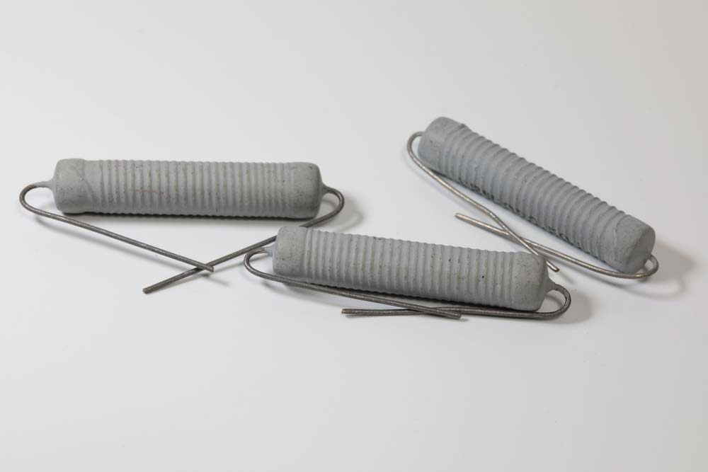
Wirewound vs Metal Film Resistor: Which is Better?

PCB Drill Sizes-A Remarkable Informative Introducing

Carbon Film Resistor VS Metal Film – How to Tell the Difference

Helping You Optimize the Thermal Profile of Your PCB
Transparent PCB: The New Generation of Flexible Circuit Boards

ENEPIG vs. ENIG: Which is the Better Surface Finish?

PCB Overmold: What You Need to Know

Polyimide PCB: Types, Applications, and Benefits

Black Pad: How to Avoid it on your PCB

What is Flux & Why is it so Important?

TQFP vs LQFP: Comprehensive Comparison of Quad Flat Packages

IC Packaging: How Should We Choose Different Types of IC Packaging?

PCB Pins-How To Use It(Latest)

Through-Hole – Why It is Still Relevant in PCB Designs?

PCB Panelization Design Guidelines

PCB Temperature: A Guide to How to Manage High Temperatures

Wave Soldering: What Is It and How It Works?

FFC vs FPC: What’s The Difference Between FFC and FPC?

Masking PCB: How and Why It’s Done

Solder Joint: The Common Defects That Exist

Solder Melting Temperature: What Is Appropriate?

PCB Assembly Express-How To Get A Valuable Service
Consumer Electronics Manufacturing Industry Overview

Flex PCB Manufacturer in China
PCB Manufacturer China: Useful Tips for Selecting One

10 Common PCB Quality Problems You Should Know

Computer Buses: An Introduction to Communication Links

How To Design Automated Light For Bed Room? (Interesting)

PCB Prototype Service – The Best Service Here

SMT Assembly-Valuable Information Introducing

The Most Detailed Introduction AOI Inspection(Latest)

One-Stop PCB Assembly Of WellPCB Introducing

PCB Holder for Easy Soldering(Latest)

How To Create A Simple Circuit Board Drawing

How to Make a Silk Screen(An Easy Way)

PCB Manufacturing Process(Simple and Useful)

Prototype PCB-How To Make It

How to Clean Flux Off PCB: A Comprehensive Guide

Fast Acting Fuse: How It’s Different from a Time Delay Fuse?

Board Stiffener: What It Is and How to Use One

Daisy Chain Routing: What it is and How to Use It

LED splitter: Installing multiple strip lights into one source!

Is Plugging Your Vias Necessary?

AOI Test – What Is Automated Optical Inspection Test?

SMT vs SMD – Ultimate Guide to PCB Assembly Terms

What are AC and DC- What is the difference?

What is a voltage divider- 4 Types of Voltage Divider Circuits

ALU PCB- Aluminum Base PCB Features and Applications

94v0 Circuit Board Diagram- Key Features and Applications

THT vs. SMD – Which Is the Better PCB Assembly Process?

Digital Sensors Examples: All You Need to Know

7 Segment Display Pins- 7 Segment Display Working and Applications

PIC32 vs. STM32: Everything You Need To Know

7812 IC – A Comprehensive Guide

Types of Inverters- Inverter Classifications and Subcategories

Night light circuit – 4 Types of Night Light Circuits

Electronic Timer Circuit – A Comprehensive Guide

Common PCB Thickness: How to Set the Right Thickness for your PCB

Simplest FM Receiver Circuit: How To Build and Use One

Pcb Antipad: Should You Use It for Your Designs?

Automatic day night on off switch – All you need to know

Li-ion charger circuit- All You need to Know

Resistive Touch Sensor: What It Is and How It Works

Wireless Charger Circuits – A Comprehensive Guide

FM transmitter circuit diagram – Full Illustrations of Various Variations

Bi-directional Amplifier- Why You Need a Bi-directional Amplifier

1n4002 diode- All you need to Know

Micro SD Pinout- Secure Digital Memory Cards Guide

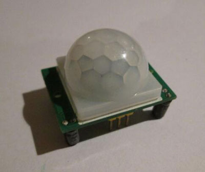
Motion Sensors Circuits – 5 DIY Ways of Building a Motion Detector
OV2640 – The Ultimate Guide on the Image Sensor

Micro amp Meter – Basic Working Principle

Prepreg vs. Pore- A Comparative Guide on Prepreg and PCB Core

NiMH Battery Charger Circuit – Features, Charging, and Working

PCB Inductor – Definition and Methods of Computing Inductance Value

FR1 PCB: How is it different from FR2, FR3, and FR4 PCBs

DIY Remote Control: How to Build One Easily

Constant Current Source – A Comprehensive Guide on Constructing Different Constant Current Circuit Designs

Do Capacitors Have Polarity – How Will You Tell?

10 Layer PCB Manufacturer: How to Choose the Right One for Your Project

Double Throw Relay – Working, Circuit Diagram, and Usage

What is Silkscreen: A Great Way to Guide Component Placement

Embedded PCB: The Perfect Board for Embedded Systems

ATMEGA8 Pinout: How to Get the Best Out of This Microcontroller
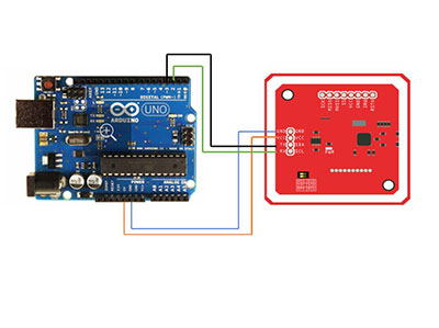
Interfacing PN532 with Arduino – Here’s All You Need to Know

Copper Clad PCB – What Is Copper Clad Laminate (CCL)?

OSP PCB: An Effective PCB Surface Finish

Microwave PCB: The Best PCB Design for High Frequencies

8 Layer PCB Manufacturer– Everything You Need to Know
Data Bus: The Powerful Subsystem for Data Transfer

Bluetooth Communication Protocol – The Ultimate Protocol Guide for Learners

Arduino Pro Mini vs Nano – A Comprehensive Comparison

PCB Designs: A Comprehensive Guide to Basic Design Steps and Rules

High Current PCB: The Perfect Board for High Current Applications

433MHz: An All-Inclusive Guide to the Wireless Radio Band

IMS PCB: The Super Heat-Resistant Circuit Board

LM324 Circuits: Different Circuits You Can Make with the LM324

STK500: A Great Way to Program Microcontrollers

k3ng Keyer: Explanation on the Arduino bases Morse Code

Can Bus Shield: Understanding All About this Automotive Controller

STM32 Nucleo: The Features and How To Connect It to Your PC

Atmega328p vs Atmega328- Features, Differences, and Similarities

PCB Track Width: How to Calculate and Optimize PCB Trace Width

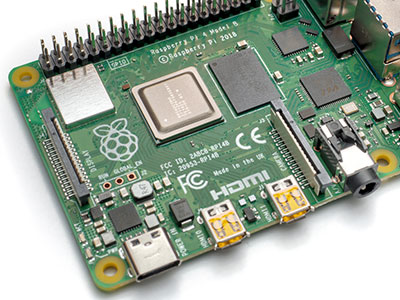
Raspberry Pi Voice Recognition: An Easy Voice Recognition Project

Temperature Controller Circuit: What Makes it Tick?

Introducing Automotive PCB: The Key to a Smooth-Running Vehicle

Arduino Alternative: A List of Other Great Options Available

SMT Machine: The Modern Way to Assemble Electronics

Zig Bee Module: An Insight Into the Wireless Device

Arduino Battery Capacity Tester: How It Works and Why You Need One
IR2104: Understanding All About This MOSFET Driver
LM311 Equivalent: The Ultimate Guide
AT89c51 Microcontroller: Programming, Pinout, Features, and Alternatives
DS18B20 1-Wire Digital Temperature Sensor – Pinout, Features, and Applications
Compute Module: What It Is and Why You Need the Board

TTL vs rs232- Differences, Upsides, and Downsides
6 Layer PCB Manufacturer With Stack up Types

HT12E Datasheet: A Concise Guide on the Encoder IC
Rk3399: Everything You Need to Know About It
nrf51822 Arduino: A Guide on Features, Applications, Advantages, and Project Example of BLE Technology
DIY Thermal Imaging Camera: How to build a Less-Expensive One

OSP vs ENIG: A Guide About How Each Work
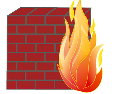
Ipfire vs Pfsense: Which Firewall Should You Choose?
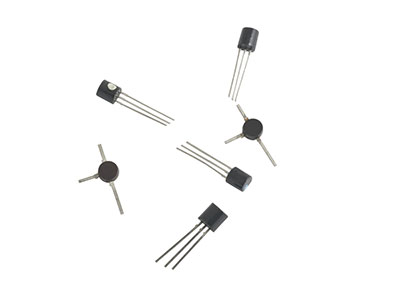
Types of Transistors: A Comprehensive Guide

AD9850 Module: A detailed Guide
Colpitts Oscillator: Circuit Application and Its Advantages
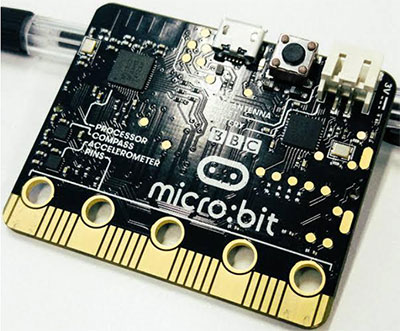
Micro: Bit Projects: 11 Cool Projects for Beginners

Motionless Electromagnetic Generator: A Guide on Designing a MEG Circuit
CH304G: The Features, Applications, and Schematic
Microwave Sensor: What It Is, Types, & the Working Principle

Solar Panels for Hobby Projects; Best DIY Solar Projects
NOOBS vs Raspbian: What Are the Major Differences Between Them?
Attiny84 Datasheet: Its Pin Configuration and Programming Steps

CD4012: Why This Logic Gate IC is Unique
Uln2003 pinout: A Comprehensive Guide on ULN2003 IC Datasheet

Flexible VS Rigid: The Differences in the Circuit Board Assemblies
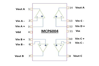
MCP6004 Datasheet – A Look Into the Low Power Quad Op-Amp
CD4027- A Complete User Guide

Hc06 Datasheet: Introduction to Pinout, Features, Applications, and Working Principle
CD4013: Basic Guide on Pinout, Application Circuit
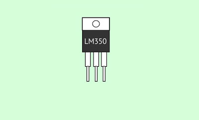
LM350 – A Complete Guide on Voltage Regulation
Capacitive Voltage Divider: An In-depth Guide
TIP31C Pinout: Technical Knowledge of the NPN Transistor
LM7805 Circuit: Voltage Regulator IC Overview
TDA2822- A Complete Guide
LM1875: A Comprehensive Guide on Audio Amplification
HT12D: A Guide on an RF Decoder IC for Remote Control Applications

S-Video to RCA Cables: Getting the Most Out of Your Connections
Tip122 Pinout: Guide to What It is, Features, and How to Use It
7815 voltage regulator: Detailed Guide on How to Use It And More!
BC547: Transistor Explained

DMOS Transistor: Its Capabilities and Structures Explained
AGC Circuit: A Comprehensive Overview
BJT Biasing: Everything You Need to Know
PCB Laminates: A Comprehensive Guide
BC558 Transistor: Everything You Need to Know
LM335 Temperature Sensor: Configuration, Specifications, and Applications

CD4066: Features, Working Principle, and Applications

Mg996r: A Brief Introduction into Its Working and Applications

Silicon Circuit Board: Benefits and How to Design One

Phone Circuit: The Basic Components and How It Works

LM7824: Description, Specs, Applications, Pinout
Sg3524 Modulator IC: Pin Configuration, Specifications, And its Application

2600mAh Battery: Working, Specifications, Application Circuit, and Other Useful Knowledge
CD4060: Ultimate Guide for its Circuits, Operation, and More!

Cold Electricity: Ultimate Guide on the Basics
LM723 Circuit: A Detailed Information on the Voltage Regulator

1n4148 Diode Equivalent- All You Need to Know

Types of DAC: Basics on Digital to Analog Converter ICS

UC3844: A Complete Guide to Everything you Need to Know

DTV Antennas: Types, Installation, and How to Make One

LM393: Pinout, Features, Applications, and Working Principle

Irf740: A Complete Guide and More!

AMS1117 Pinout: The Best Guide for Beginners

AM Receiver Circuit: Understanding and Building A Simple Project with It

Center-Tapped Transformers: A Brief Introduction into Its Working and Applications

IRFZ44N: A Complete Guide on Using This MOSFET

Crystal Oscillator Circuit: How to Build One

ERP Radio: What Is It and What Factors Affect It?

Potentiometer Wiring – Process Simplified

SCR Bt151: A Complete Manual Guide

X Rated Capacitor: How to Use One in a Transformerless Power Supply

Yagi Antenna Design Formula: Understanding its Parasitic Elements and More!

Brushless Motor Wiring: Its Specifications and Complete Guide!

Emitter Follower Circuit: The Basics and How to Create One

Start Stop Circuits- A Brief Introduction Into Its Components, Working, And Control

Low Voltage Cutoff Circuit: The Working Principle and How to Make One

Blocking Oscillators: An Introduction Into its Working, Types, and Uses

2SC2879: Everything you Need to Know and More!

Overvoltage Protection Circuit: Meaning, Types, and DIY Projects Explained

Battery Backup Circuit: A Comprehensive Guide in Making One

Speaker Crossover Wiring Diagram: The Types and How to Build the Network Circuit

Water Detector Circuit- Working Principle and Basics

Notch Filter Design: A Narrow Band Filter for Specific Noise Attenuation
Electronic Circuits for Beginners: The Complete Guide
Microcontrollers Basics: The Structure, Working Principle, and Applications

Homemade Car Alarm: The Benefits and How to Make the Device

Relay Drive; Definition, Working Principle, and Application Circuits

Dpdt Relay: The Complete Guide

Metal Detector Circuit: An Introduction Guide

Voltage Doubler: A Cheaper and Lighter Alternative to Transformer-Rectifier Circuits

Input Impedance of Op Amp: What It Is and How to Calculate It

Negative Edge Triggered Flip-Flops: Basic Electronic Knowledge

4047 IC: A Detailed Introduction To A Monostable and Astable Multivibrator

Log Amplifier – All Important Information to Know

LM338 Circuit: Detailed Datasheet and Application Circuits

Transistor Flip Flop: A Sequential Logic Circuit for Storing Binary Data

CD4049: The Features, Applications, and Circuit Diagram

Fish Stunner Circuit Diagram: How it Works and the Simple Build Steps

24v to 12v Converter Circuit: Circuit Diagrams and More

NE5532 Preamp Circuit: Building Different Circuits with This Audio Amplifier IC
Ultrasonic Fogger Circuit: A Start to Finish Guide
Class C amplifiers: A Complete Guide and More!
Heat Sensor Circuit: Operation and How to Build One

556 Circuits: Ultimate Guide for its Operation

Beaglebone Black Pinout: Pin Configuration, Specification, and Application

SPDT Switch Wiring: Everything You Need To Know

Passive Tone Control Circuit: Applications, Design, and Benefits

Air-Core Inductor Design: All You Need to Know

DIY Thermoelectric Generators: The Working Principle and How to Make One

Voltmeter IC: A voltage measuring tool

Trimpot Pinout: Understanding the Features, Uses, and Configuration.

LDO Circuit: The Basics, Working Principle, and Applications

DHT22 Pinout: How it Works and its Application

DIY Ultrasonic Dog Repeller: Keeping Canines Away

MOSFET Protection: How to Properly Protect It

How Does a MOSFET Work: Basic Understanding, Types, and Applications

DIY Logic Probe: Step by Step Guide

Resistor Circuit Diagrams: Understanding Connections and functions

Raspberry Pi Camera Pinout: What It Is and How to Use It

High Current Voltage Regulator: The Definitive Guide

Touch Lamp Circuit: A Comprehensive Guide

Heart Rate Monitor Circuit: A Well-Detailed Guide

Automatic Voltage Regulator Project: Designing and Constructing Your Very Own Circuit

lm386 Amp: Everything You Need to Know

Clapp Oscillator: Circuit Diagram, Frequency, Advantages, and its Applications

IRF3205: A Guide through the N-Channel MOSFET Datasheet

Transistor Saturated: What It Is and How to Identify One

Clap Switch: An Easy Project for Beginners

Ultrasonic Sensor Circuit: A Complete Guide

Isd1820: A Voice Recorder Module Guide

Audio Circuit Mixer: 5 Ways of Building an Audio Mixer

Ferrite Core Transformer: A Definitive Guide on the Basics

Audio Delay Circuit: Creating Echo and Reverberation Effect in Audio

VFD Schematic: VFD Circuit Diagrams, Types, and How to Build One

FET Test: How It Works and When It’s Needed

Potentiometer Circuit: How They Work and What They Are Used For

USB Pinout Guide: Everything You Need to Know About USB Types and Pinouts (2024)

DIY RFID Reader: How to Make One That Works Effectively

Replace Transistor – How to Make the Best Choice

Alarm Circuit: The Construction and Working Principle

Tachometer Circuit: How it Works and How to Make One

8 Channel Relay: Everything You Need to Know

Types of Inductors: The Ultimate Guide
Bd139 Pinout: The Only Comprehensive Technical Guide You’ll Ever Need

2N3819: The Ultimate Guide

Variable Voltage and Current Power Supply Circuit- High-quality Variable Stable Output

Bluetooth Interfacing: How to Interface With Bluetooth Modules

AM Loop Antenna: Everything You Need to Know About It

Neon Lamp Circuit: What Is It and How It Works?

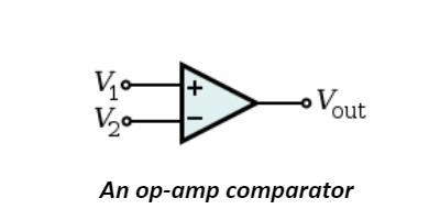
Opamps Hysteresis: The Ultimate Guide

IC 4060: Understanding the Pinout and their Functions

Continuity Tester Circuit: How to Build a Simple Continuity Tester

How to Make a 12 volt Battery: A Short and Clear Guide

Voice Changer Circuit: Building a Voice Modulator Circuit

AM Radio Schematic: A Guideline on Making Simple Circuit Diagrams
Transformerless Inverter -All You Need to Know

Ripple Carry Adder: Everything You Need to Know

How Does Piezoelectric Work: A Complete Ultimate Guide

Tantalum Capacitor Marking – Understanding the Fundamentals of Capacitor Marking and Types

Refrigerator Alarm: What Is It and How It Works?

Circuits With Free Energy: Is it Possible to Make Free Energy?

DIY ESR Meter: Everything You Should Know About a DIY ESR Meter

Transistor Latch: A Comprehensive Guide That Explains Everything

BJT Load line: A Better Understanding of The Function

Noise Filter Circuit: Improving the Sound on your Listening Device

RTOS vs GPOS: A Complete Guide

Hypersonic Sound System: The Complete Guide for HSS

74LS47: Understanding The 74LS47 Data In Details

Tip120: Basics on TIP120 Transistor

4017:IC 4017 Specifics and Configurations

Analog vs. Digital Oscilloscope: What’s The Difference?

555 Oneshot Circuit: Understanding Monostable Designs

Types of Fuses: The Ultimate Guide for Fuses

Digital Buffer – A Comprehensive Guide

DIY Digital Analog Converter: The Complete Guide

What Is a MOV: Metal Oxide Varistor Tutorial

Transformerless Power Supply: The General Basics, Working, and Requirements Explained

TRIAC Symbols: A Comprehensive Guide for Beginners

Varistor Symbols: A Complete Guide On Its Working and Applications

DIY Solder Iron: The Homemade Solder Iron Guide

UPS Circuit: Everything You Need To Know and More

What is SCR: Everything You Need to Know
TL494: Everything You Need to Know For Your Project

How to Make a Rectifier: A Detailed Guide

DIY Walkie Talkie: A Complete Step-by-Step Guide

Farady Flashlight: Everything You Need to Know

Test a MOSFET – How to Conduct an Effective Test

Remote Control Car Circuit: Everything You Should Know About It

Volume Control Circuit for Speaker: Step by Step Guide to Enjoy Your Music

How to Build a Radio Repeater: A Complete Guide

Top 6 Methods to Convert Three-Phase to Single-Phase Power: A Step-by-Step Guide

Transistors in Parallel – The Ultimate Guide and Avoiding Mistakes

Buzzer Circuit: How to Create and Enhance an Easy Design

Transistor vs Resistor: What’s The Difference?

Battery Desulfator Circuit: A perfect solution for battery failure

Taser Circuit – The Best Self-protection Device and How to Build One

DIY Battery Chargers: The Complete Guide

Resistor Values: How to Calculate and Understand It

IC4017: A Beginner’s Complete Guide

Self-Powering Generators: A Must-have Guide for the electronics industry

Timing Delay Circuit: Explaining a Time Delay Circuitry and its Applications!

Inverter Circuit: The Ultimate Guide to Making Circuits at Home

DIY Float Switch: Everything You Need to Know

Flexible Resistor: Everything You Need to Know

LED PCB -The Most Useful Introduction

PCB Milling: How To Make

Circuit Board Components And What They Do

China PCB Assembly-The Most Important Aspect

How To Design A PCB Layout(Helpful)

How To Make Power Bank Circuit On PCB

Designing PCBs – How To Solve The Problems Encountered?


Power Supply Noise Decoupling in PCB Design

PCB manufacturing

PCB Manufacturers Online-Helpful Introducing

How To Use LM386 Audio Amplifier Circuit Effectively

PCB Wiring-How To( Easy Methods)

Vias and Traces – How Conductive on the PCB?

Pick And Place-How To Do The Basics Of PCB Design

SMT Stencil-How To Make Holes In

SMD – The Best Guide to SMDs and the SMT Technology
With the leaps and bounds experienced in this industry, various technologies come in place to manufacture these devices, and the Surface Mount Tech...

PCB Hole Size-How To Drill It-Quickly Review

How To Make The Etching PCBs

Desoldering Pump-How To Use It?
Right until now, you might have heard about the Solder sucker, and it is not just ringing a bell. The Solder sucker is commonly referred to as the ...

32-Layer Printed Circuit Boards: Techniques, Applications, and Benefits

Photolithography Technology – The Most Useful Introduction

Desoldering and Solder Removal Techniques: The Ultimate Guide

Printed Circuit Board Design-How To Make It Wonderful

Custom PCB Design-How To Better

Integrated Circuit Systems Ultimate Guide

IP20 Devices: Introducing The IP Rating System

Spray Silicone Sealer: Your Right Choice for Electronics Application

Thermal Adhesive: Bonding Electronic Components

LED circuit board: 7 things you need to know

Fiducial PCB: Design and Function

PCB Plating: The Complete Guide of Plating Techniques in PCB

PCB Layers: The Ultimate FAQ Guide

Lead-free solder vs. Lead solder: A Comprehensive Guide You Should Know

Aluminum PCBs: What Is It and Why You Need It?

How to Solder – A Complete Beginner’s Guide to PCB Soldering
Understanding how to PCB soldering your circuit board properly can be an exc...
10 Guidelines to Help You Successfully Flex PCB Soldering

8 Special Steps in Rigid-Flex PCB Manufacturing Process

7 Important Factors of PCB Conformal Coating Ideal Thickness
A conformal coating is a fragile polymeric...

6 Tips for Affordable Small Batch Assembly
A majority of PCB assemblers, especially small-batch manufacturers that are just starting t...

9 Ways to Get BGA Soldering on PCB in SMT Assembly
When it comes to SMT assembly, you may hear of people talking about BGAs or Ball Grid Array...

HASL VS ENIG: 10 Tips on How to Choose Enig Plating
Selecting the right surface finish for your printed circuit boards is as essential as finding a manufacturer to produce the Read More

10 Tips to Consider When Converting a Schematic to PCB Layout
PCB manufacturing is a multi-step process. Each stage of the process is equally import...

9 Common PCB Soldering Defects and Solutions
For more than two decades and counting, wave soldering has been relied upon by PCB designers for Read More

Custom PCB Printing-6 Things You Should Pay Special Attention
Printed circuit boards are indispensable units in nearly all electronic products that ...

5 Ways to Order Custom Printed Circuit Board Online

PCB Components- 14 Important Tips for Choosing PCB Components

How the PCB Component List Can Make or Break PCB
A well-planned and thorough bill of materials is highly essential to the proper functioning of a circuit in addition to maximizing a manufacturer’s...

Conformal Coating PCB: 7 Reasons Why You Need It
A conformal coating PCB that is a protective material that you can apply to the printed circuit boards when the assembly process is in the fin...

7 Ways to Balance Electronics Manufacturing Cost and Performance
Every buyer wants to get low-cost high but high-quality products for themselves. But does expensive mean better high-quality products? To a more co...

13 Tips and Technology to Know About Printed Circuit Board Assembly
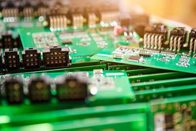
When you see these boards, most people can recognize them. They are green and made of copper, and you can find them in electronics. The assembly pr...

7 Problems in the Multilayer PCB Fabrication Process
Printed circuit boards, also known as PCBs, in short, are what make all electronics to function as desired. Therefore, when something goes wrong on...

9 Ways to Reduce Costs in Multilayer PCB Manufacturing
When ordering multilayer printed circuit boards, it is essential to ensure that you purchase them at reasonable costs. However, a majority of custo...

7 Tips to Prepare Printed Circuit Board Assembly Documentation
Upon the completion of the design process, it is essential to give it to the appropriate PCB supplier. Then it is necessary to provide the complete...

10 Things You Need to Know About PCB Assembly Costs
PCB assembly cost include the cost of labor, turnaround time, technology, and the quantity of PCBs needed. Technicians and engineers alike often wo...

9 Years of Experience Tell You That Big Trap of Cheap PCB
Every one of us desires to save a little buck, and many people, when looking to save some cash, focus on finding some of the most affordable deals ...

5 Ways To Get a Low-Cost Printed Circuit Board Quote
Printed circuit boards are a bit expensive, and it is always good to spend some signif...

10 Tips to Choose the Right Flex Circuit Manufacturer

8 Ways to Optimize Circuit Board Assembly Speed
7 Reasons for Businesses Turning To Small-Batch PCB Manufacturers

10 Factors to Achieve Low-Cost PCB In China

7 Most Common Cheap PCB Manufacturing Defects and Solutions

10 Comparison Aspects Of Rigid and Flex PCB

9 Tips To Help You Find The Cheapest PCB Manufacturer

9 Useful Ways To Help Build a Custom PCB Easier

Big Advantages of China PCB Manufacturer

A Comprehensive Guide To Building Digital Circuits

How To Determine the Number of Layers of Multilayer PCB?

How to design a professional and beautiful Circuit Board Pattern

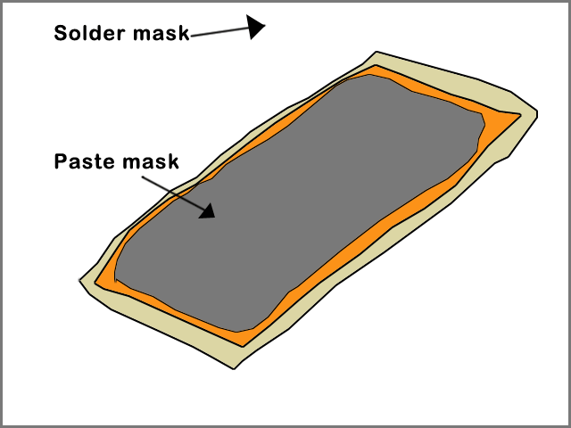
6 Steps To Understand The Solder Mask

A Simple Guide to Electronic Components

Flexible Rigid PCB – How to Make its Assembly Look Simpler And More Reliable

How to Determine if Your Product is HDI or A Regular PCB Board

Whether HDI PCB Can Meet Your Needs, Here Are the Answers!

Flex PCB Assembly-How to Get a Wonderful PCB
Rogers PCB – The Ideal Component for Efficient Circuit Boards

Flexible Flat Cable – How to Make your Designs More Innovative?

Edge Connector Beveling-Gold Finger Plating for Edge Connectors

Wearable Electronics-Ultimate Guide On Wearable Technology

Conductive vs. Non-Conductive Via Fill PCB

Presensitized PCB: An Ultimate Guide

Bom File – How to Designe a Bill of Materials for PCBA Manufacutring

Rigid-Flex PCB-How to Streamline and Improve Reliability

Standard PCB Drill Sizes-Tips You Should Know

Multilayer PCBs – How are they better or worse for you?

Low Volume PCB Assembly Process Ultimate Guide

10 Awesome Advantages of Rapid PCB Prototyping Service

Ultimate Guide to PCB Design and Manufacturing

Surface Mount Soldering-A Comprehensive Understanding of Soldering

PCB File-How To Make Your Files High Availability

Single-Sided PCB – The Ultimate Guide to How to Save More

PCB Art- The Ultimate Guide to How PCBs Are Better

PCB Assembly Process-9 Tips On How To Ensure a Smooth PCB Assembly Process

Ultiboard – The Ultimate Guide For Best For Beginners

Bare PCB-Simply Know About It’s Technology

10 Tips for Choosing the Right PCB Manufacturer and Supplier in China

Quick Turn PCB-Ultimate Guide On How To Get Your PCB

PCB Stencils-The Ultimate Guide On How To Make It

PCB Assembly – How To Be More Professional

NRE Cost – How To Make the Project Perfect

PCB Troubleshooting-Ultimate Guide On Purpose And Problems Goal

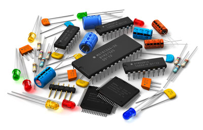
Integrated Circuits: An In‐Depth Guide

PS4 Controller PCB Circuit Board – What You Need to Know

How To Remove Solder? (Improved Way)

Sprint-Layout – The Ultimate Tutorial And Experience

White PCB – An In-Depth Guide About It

94V-0 Circuit Board – The Ultimate Guide Is Here

PCB Material-(Selection requirement while designing the PCB)
Solder Mask – The Most Comprehensive Introduction Is Here

Flexible PCB Prototype Manufacturing Services

A Guide to Moving from Breadboard PCB Prototypes to Full Product

PCB Trace Thickness: What You Should Know

How to Repair Circuit Board

Mylar Boards-How To Do With It

PC Boards-Manufacturing Tips Ultimate Guide

PCB Cleaning-How To Clean Your PCB

PCB Mounting-Easily Install Guidance It’s Here

Flex PCB-How To Manufacturing And Use

Flex PCB Manufacturer-Valuable And Useful Introducing

PCB Substrate-What You Should Know About It

Flexible Quote For Manufacturing Flexible PCBs

Multilayer PCB Demands and Requirements Pertaining

PCB Manufacturing Equipment-Important And Valuable

Flex PCB Prototype-How To Make It
