Contents
PCB Troubleshooting
Overview of PCB Troubleshooting
The quality of a PBC device hinges on the degree of precision with which it dispenses its functions. But the human inputs in its fabrication processes can engender Trojan horses.
Sheer human errors are usually the root causes of defects in PBCs. Some of these errors include components soldered wrongly, the use of inappropriate voltages, etc. However, there are a number of other defects that are not direct results of human error, such as component degradation.
But a common thing about both sets of errors is that most of these defects are usually difficult to decipher. In such instances, troubleshooting techniques help you unlock insights.
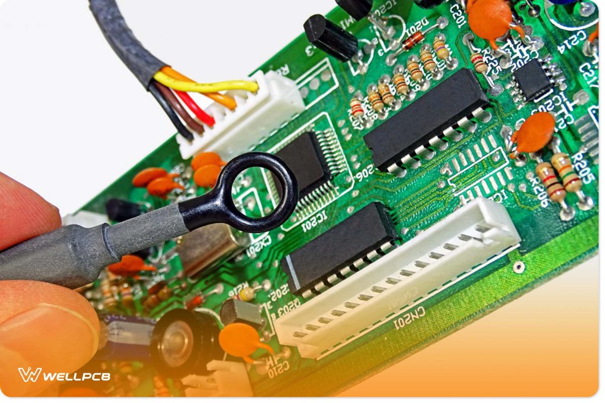
The Scope of Issues Which PCB Troubleshooting Deals With
The operations of PCB electronics revolve around electricity, which is the flow of electrons from one level to another. The functions of PCB electronics are based on the regulation of voltage and currents within the circuit board.
The elements that imbue a PCB electronic with such regulatory attributes include resistors, capacitors, inductors, and soldered wiring. However, damages due to voltage spikes and over-current torrents can disrupt the pattern of electron flow in the board.
Most of the defects resulting from such disruptions are known as intermittent failures.
Which Troubleshooting Technique Is the Most Effective in a Given Case
The number of layers, the size, the range of components, etc., influence the viability of a PBC troubleshooting technique used. Highly sophisticated boards will most likely require you to troubleshoot using special equipment.
However, basic electrical equipment will help you successfully troubleshoot PBCs most of the time. That’s because, generally, PBCs are quite easy to troubleshoot. You’ll, therefore, find it easy to troubleshoot an average PBC without the use of advanced tools.
One of the most dynamic tools for troubleshooting PCBs is the multimeter. However, in highly complex cases, you may need to use advanced equipment such as a logic analyzer, an oscilloscope, and an LCR meter.
These tools unlock insights into a PCB’s operational behaviors and mapping.
Interested in learning more about how troubleshooting tools reveal PBC mapping and operations? The next chapter delves into this.
PCB Mapping
The Importance of PCB Mapping in PCB Troubleshooting
A typical PCB board consists of a network of copper traces and insulators that connect clusters of components in a circuit board. One of the reasons why some PCBs are easy to troubleshoot than others is the availability of the PCB’s schematic.
It’s easier to troubleshoot a PCB if you already have a clear understanding of its current flow, signals, and traces. It’s essential for you to know which capacitor pairs with which resistor to troubleshoot.
Understanding the position of the voltage divider, filter and choke in the PCB is also essential, but if you don’t understand a PCB’s configuration, it’s best to troubleshoot beginning with the connectors.
The connectors are the interface from which erroneous inputs from the external environment make their way into the PCB. Such erroneous inputs can result in voltage spikes, over-current torrents and the like. However, you need to be well-versed in mapping a PCB to troubleshoot without access to the board’s schematics. If you’re not, it might take a long time to trace the configuration of the PCB.

How to Map Out a PCB
One way to begin trouble troubleshooting without understanding the PCB’s schematics is to use standard multimeter probes. However, this might be tedious, as you’ll need to test every solder joint with the multimeter probe.
However, a more natural way to trace out the PCB is by using a piece of aluminum. This technique allows you to search for PBC connections over a wider area per time, minimizing time and effort. To do this, you need a multimeter, wires with crocodile clips, a piece of aluminum foil, and a wire cutter.
Start by stripping 2cm of the wire at one end and 4-5 cm at the other end. Wrap the piece of aluminum foil around the wire. Then, connect the foil’s cable to the multimeter’s wire. Wrap the foil around one of your fingers, and then touch the second multimeter wire with that finger.
It would help if you were getting a 0 ohms resistance measurement. However, if the reading is above 15-20 ohms, you need to carry out the foiling operation again.
After successful completion, use the multimeter’s probe to touch the board at one location at a time. Therefore, place your finger on the foil and touch the welded part of the assembly. This way, you can quickly cover more areas. When the multimeter beeps, that means you’ve found a track connecting the components.
Now that you know a whole lot about PCB mapping, you should be primed to learn the troubleshooting steps.
How To Troubleshoot
Here are some of the crucial steps you need to take first when troubleshooting a PBC:
Visual Inspection
Conduct a visual inspection of the board to identify burnt components, cracks, and dry joints. This is one of the easiest ways to troubleshoot without power.
A good magnifying glass is a crucial tool for visual inspection, as there may be some little physical damage.
You’ll get to learn more about visual inspection in the subsequent chapters.
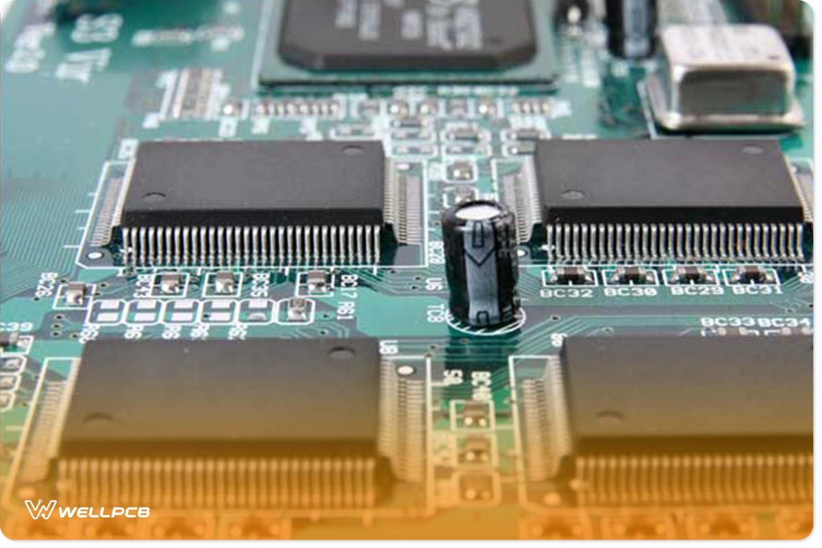
Physical Inspection of Power Supply
If the visual inspection does not lead to any significant findings, then it’s time to check the power supply. You need to ensure that the integrated circuit (IC) receives the appropriate levels of the power supply.
Inappropriate levels of power supply to the IC can cause overheating or overloading on the board. You can easily trace where high voltages might have caused damage by merely touching the PBC’s surface and components.
By touching various parts of the circuit, you also alter the impedance of the circuit. So, since this alters the system’s behaviors, it can help you trace out the parts that need additional capacitance.
You can use compressed canned air to cool a hotspot to test if the component is functioning correctly. However, you need to take some precautions while doing this.
One precaution you should take during physical inspection is ensuring that you touch the PBC with one hand per time. That prevents electrical jolts from reaching the heart to cause fatal shocks. A good practice is to keep one hand in your pocket while touching a live circuit.
Another critical precaution is blocking out any potential path to the ground for the current to prevent shocks. These paths include your bare feet, as well as a non-resist grounding strap.
Explicit Component Testing
That is the stage of troubleshooting where you’ll need to start using test tools. First, you need to measure the power supply voltages in the entire board.
Afterward, measure the voltages at various parts of the circuit to identify any part with inappropriate voltages. The circuit diagram will come in handy at this stage.
Now that you know some of the necessary steps for troubleshooting PBCs, you might want to know what’s the best step. Find out the best PBC troubleshooting steps in the next chapter.
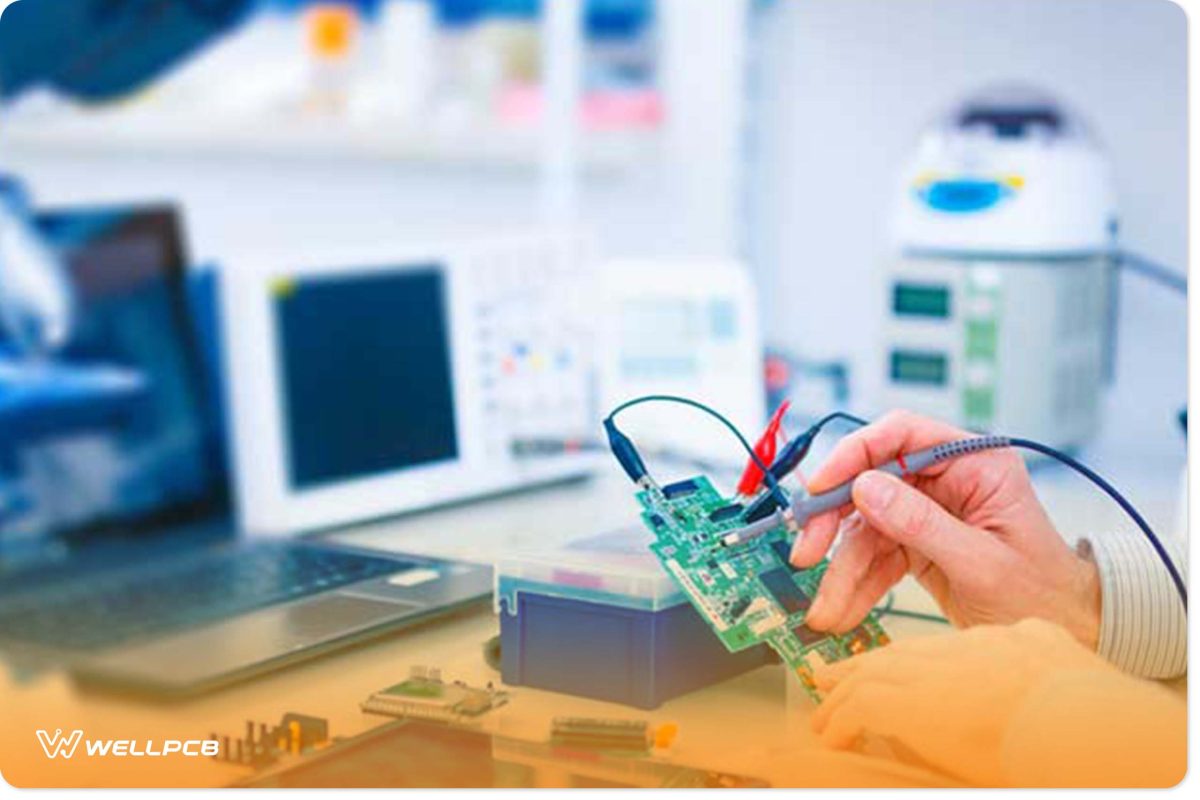
The Best Ways To Troubleshoot PCBs
Nodal analysis
The best PCB troubleshooting technique is testing the components using nodal analysis. This technique allows you to test PCBs without powering the board. You only need to apply power to the particular component you want to test per time. The aim is to measure the applied voltage and the current response of the component.
Nodal analysis entails systematically measuring the voltages at specific nodes to compare them with the voltage of a reference node. This reference node is randomly selected from the various nodes on the board. The technique entails applying the KCL to determine the difference between the voltages of the nodes in branch currents terms.
The difference between the nodal voltages is determined by a system of equations that describe the circuit’s operations. You can quickly determine the current response at a node once you’ve figured out the equation.
There will be a total of N-1 independent equations yielding node voltages since one node serves as the reference node. You can then apply Ohm’s law to the measured node voltages to decipher the currents in the circuit.
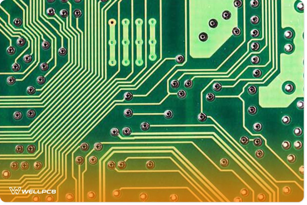
How to Implement Nodal Analysis
1. Identify the number of nodes, then choose and label the reference node. The rule of thumb is to select a node that connects the most significant number of elements or voltage sources or asymmetrical nodes.
2. Assign each of the unknown voltages of a node with a variable. So then express the unknown voltage to the known voltages.
3. Write down equations that express the value of secondary sources regarding node voltages.
4. Write a KCL equation for every node by reducing the out-flowing current of the node to zero. The KCL holds that the algebraic sum of all currents flowing in and out of a node equals zero. Use the KCL to determine the unknown variables.
5. For voltage sources between two unknown voltages, combine the two nodes into a supernode and express it in a single equation.
PCB Problems And How To Fix Them
Errors are almost inevitable in the design and manufacturing processes of PBCs. However, these problems are common problems that you can quickly resolve. The following is a rundown of the three most common problems and how you can overcome them:
Defective Copper-to-Edge Clearance
Copper has excellent conductive properties. However, it is usually coated with other materials because it’s easily susceptible to corrosion and wear.
However, during trimming, the coating on a copper fitting that’s close to the edge might be shaved off. It can result in numerous defects in the PBC electronic. This exposure can even lead to electric
shocks when someone touches the PCB directly.
An easy way around this problem is to ensure there is adequate space between the copper and the board’s edges. This space is known as copper-to-edge or plate-to-edge clearance.
Electromagnetic Interference from the Operations of Midget Relay
PBCs produce arc discharges when cutting high currents, and that gives rise to midget relays that produce electromagnetic interference. This interference can cause a CPU to reset frequently, as well as decoders that produce wrong signals.
You can resolve this problem by enhancing the anti-interference capabilities of the CPU or reducing the source of the interference.
Acid Traps
Acids fill up acute angles in a PBC during the etching process. The trapped acids might eat away at the boards and cause defects. Acid traps are very common, and they’re usually one of the main errors addressed by a DFM check.
PCB Troubleshooting Techniques
Visual Inspection
It is one of the most comfortable and most effective PCB troubleshooting techniques. It revolves around searching for brownish burn marks that result from overheated components.
Visual inspection also aims to identify lousy solder joints. A good solder joint appears typically smooth and shiny. A dull-looking joint might be indicative of a dry joint. A dry joint causes weak contact at the solder joint, altering the circuit’s conduction.
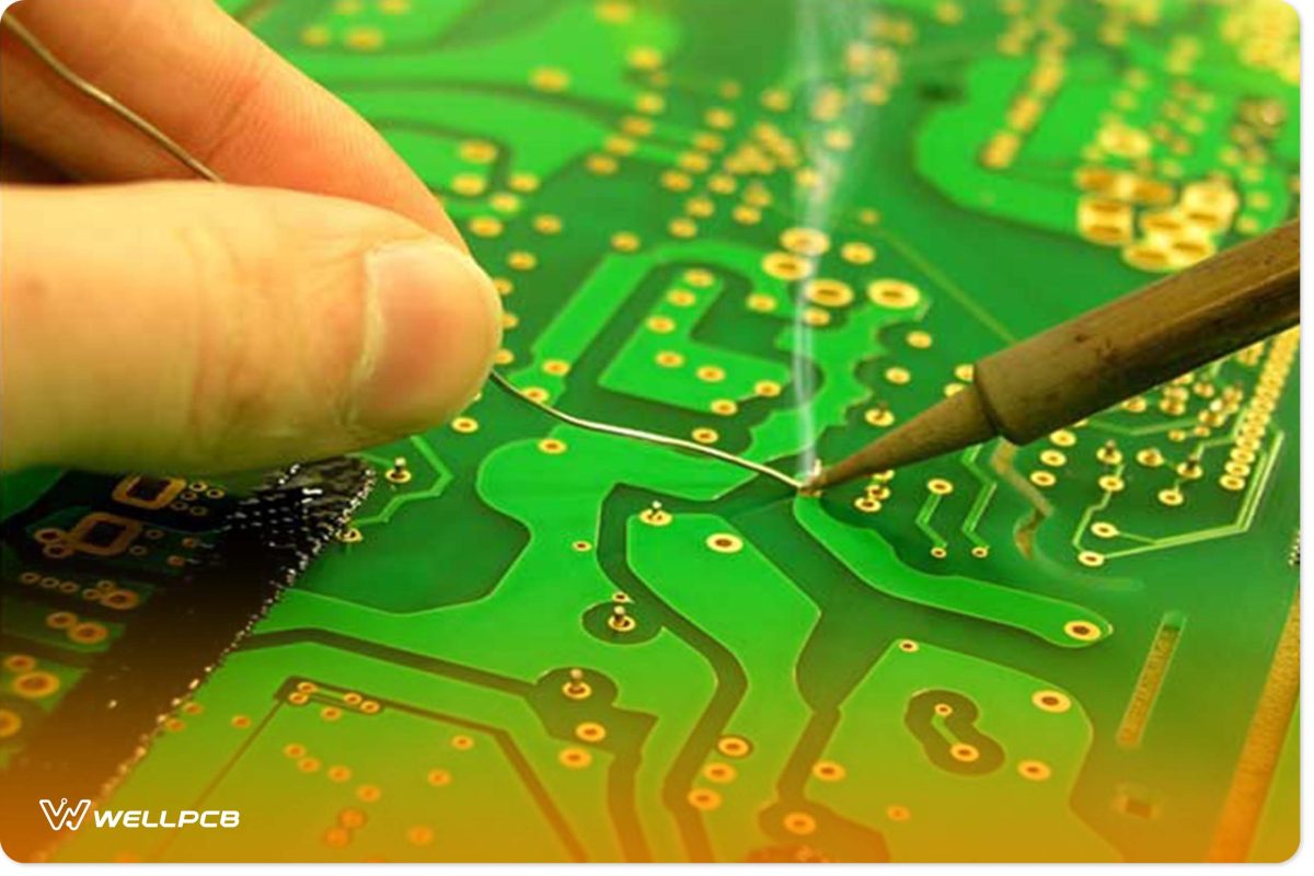
Sometimes, the dry joint and burn marks may be invisible to the naked eye. A magnifying glass can help you identify damages that elude the naked eye. A magnifying glass is, therefore, an essential PBC troubleshooting tool.
Comparing Circuit Boards
This is another quick yet highly effective PCB troubleshooting technique. It entails a quick comparison of defective circuit boards with good ones. This comparison is usually made by inspecting the reference points of both the defective and the first circuit board using a multimeter and then comparing the values obtained.
Discrete Component Testing
That is one of the most effective PCB troubleshooting techniques because it entails testing each component. These components include the capacitor, resistor, LED, diode, and other discrete active components.
You can use a multimeter or LCR meter for this troubleshooting technique. The nodal analysis method outlined earlier is also another variation of this technique.
The objective is to identify components with values that are higher than their stated component value. Such higher values usually occur as a result of overheating, lousy soldering, or an inert defect in the component.
Signal Probing
This technique requires a clear understanding of the circuity to identify the signal test point and to interpret results. Signal probing usually involves voltage tests involving the use of a handheld multimeter, as well as waveform capture involving the use of an oscilloscope.
In the voltage test, a lower voltage level indicates leakage in the integrated circuit. Waveform capture, which shows how signals change, provides you with more information than the voltage test.
Now you know a whole lot about the most widely used PCB troubleshooting techniques. However, what can you possibly achieve with all the information?
Conclusion
PCB troubleshooting requires attention to detail, determination, and focus. The most effective troubleshooting method and tools depend on the level of complexity of the PCB as well as your experience.
With a full breadth of experience, you can quickly troubleshoot nearly any kind of PCB without using advanced tools. However, if you lack the tools or expertise to troubleshoot a PCB, it is essential to contact experts in the field so as not to cause more damage.


