Contents [hide]
- 1 Definition of Through-Hole Technology
- 2 Types of plated holes
- 3 What is the role/importance of plated through-hole?
- 4 How to decompose the plated through-hole/decomposition process
- 5 Plated Through-hole Processing Equipment
- 6 Problems and Solutions of Plated Through-holes
- 6.1 Blistering and lamination on board
- 6.2 Inability to remove adhesive and oil stains
- 6.3 Neutral water is not clean after decontamination, and there is Mn on the board.
- 6.4 Surfactant on the board
- 6.5 Insufficient roughening of copper surface
- 6.6 Tin on the copper surface
- 6.7 Surface oxidation of copper foil
- 6.8 No copper in PTH
- 6.9 Unbalanced degreaser
- 6.10 PTH cylinder imbalance component
- 6.11 Over acceleration
- 6.12 The drilling roughness is too large.
- 6.13 Long-term storage after PTH
- 6.14 Fill the board with foreign matter or blister after PTH
- 6.15 Plughole
- 7 Summary
Definition of Through-Hole Technology
Before proceeding, it would be essential to understand the true meaning of through-hole technology. What is PTH technology?
Through-hole technology commonly goes by the name ‘thru-hole’ too. It’s mostly a mounting scheme for electrical components.
It includes the use of holes in the insert hole, then soldering to the PCB pad.
The insertion of components is an exercise that one can do either manually or by using an automatic insertion machine.
The through holes in a PCB undergo some plating, hence the term PTH. Plated through-holes have a conductive path moving from one side of the PCB to the other.
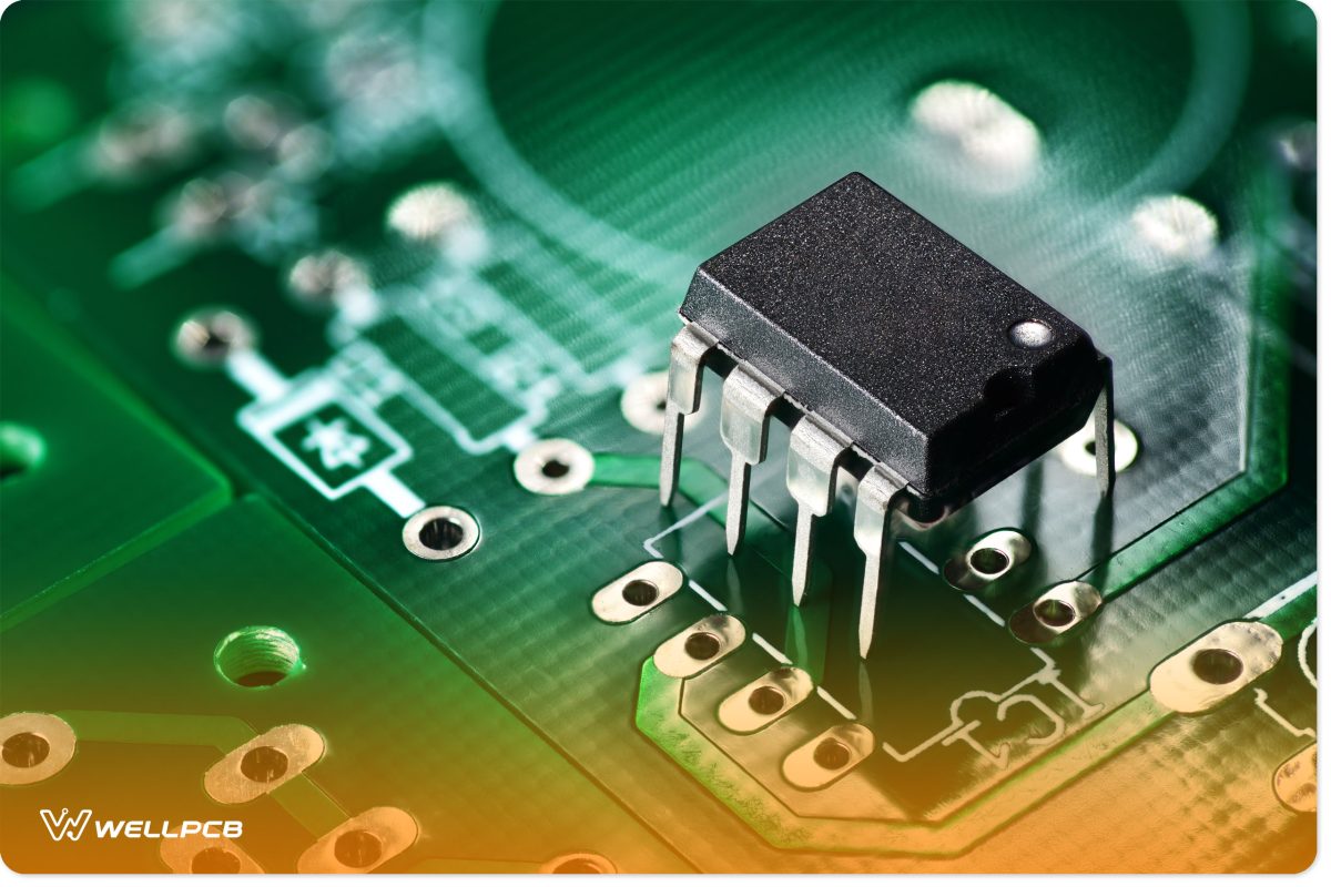
(A close picture of an electronic chip component sitting on top of through-holes)
Types of plated holes
There are several types of plated holes, as explained below:
Electroplating slot (PTH)
The primary and most notable feature of this electroplating bath (PTH) is its manufacturing process.
In its manufacturing process, after drilling the board, then plating on the hole wall. All of these are to provide them with the required conductivity.
Therefore, after the completion of PCBA, the link between the component’s leads and copper tracks achieves better mechanical stability.
Lately, a majority of PCBs tend to be double-sided or multi-layered with plated through-holes. This way, the components effectively connect to the required layers.
Non-plated slot (NPTH)
Just as the name suggests, here, there’s no copper plating on the walls of the holes. It, therefore, means that the barrel of the pickles lacks electrical properties.
These plantings were once very popular, especially when PCBs had copper tracks printed on one side. However, as the number of layers in PCBs increased, their popularity declined.
The primary advantage of NPTH is that they are relatively easy to manufacture and much faster.
While they are frequent, they don’t find exclusive use as tooling holes. But sometimes, manufacturers use them for component mounting.
The difference between them
There are notable differences between the plated through-hole (PTH) and the non-plated slot (NPTH).
The first differentiating factor is the path difference between them. All this happens on a given certain.
How waves travel in a plated-through hole is different from how they take place in a non-plated slot. Since PTH has conductive paths from one side of the board, its approach isn’t the same as that of NPTH.
Also, copper on the wall is another huge differentiating factor between the two. As noted earlier, non-plated slots don’t contain copper on the walls of the holes.
This aspect makes it lack superior electrical conductivity. But on the other hand, you’ll find copper materials on the walls of plated through-holes.
Lastly, PTH and NPTH differ in terms of applications.
Mostly, plated through-holes are heavy in providing excellent connectivity between double and multi-layer PCBs.
They are also applicable in applications that require strong physical connections. Mostly, you’ll find them in aerospace and military applications where durability is essential.
While PTH may seem old and outdated, you cannot ignore its vast applicability. On the other hand, NPTH isn’t as highly applicable as PTH.
They are ideal for single-layer boards. Therefore, their relevance is another differentiating factor between the two.
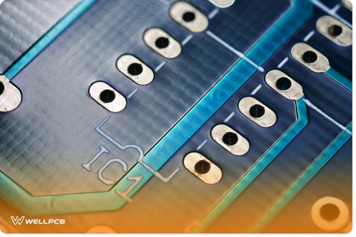
(A close picture of plated through-holes on a blue PCB)
What is the role/importance of plated through-hole?
The importance of plated through-hole, especially in modern circuitry, is crucial.
Below is a brief but also clear explanation of two critical issues—first, the importance of plating through holes on a PCB and, secondly, the importance of PTH.
Why are through holes plated on the PCB?
The plating of through-holes on a printed circuit board is to ensure the achievement of several important things.
But before proceeding, it’s crucial to understand that plated through-hole technology has achieved much.
Most importantly, it has almost done away with old electronics assembly techniques. Wire wrapping is one such example.
But why the plating of holes on a printed circuit board? Manufacturers do plating to ensure that the components make contact with the conductive layers.
A role we usually refer to as vias, the plate provides excellent electrical conductivity. For the desired functionality of a PCB, plating is necessary.
Importance of plated through-hole
A few notable advantages come with a plated through-hole. For instance, a plated through-hole gives room for faster prototyping.
Also, with a plated through-hole, it becomes more accessible to solder components on the board.
Additionally, breadboarding the design of the circuit board becomes a possibility even before board manufacture.
With plated through-holes, rest assured of component durability and high power tolerances on the board.
That’s not to forget the outstanding excellent connections that come with plating through holes. As you can see, the importance of through-hole is vast enough.
For the best solution, ensure that you source your PCBs from reliable suppliers.
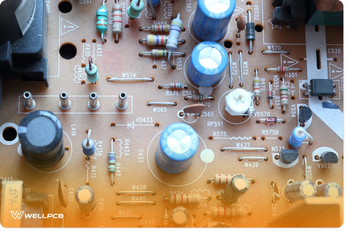
(A brown PCB with through-holes that hold several components)
How to decompose the plated through-hole/decomposition process
We can clearly understand the decomposition process for plated through-hole by referring to the diagram below:
Alkaline cleaning→ countercurrent rinsing→ roughening / micro-etching) → countercurrent rising→ pre-dip→ activating → countercurrent rising→ besmearing→ countercurrent rinsing → PTH→ countercurrent rinsing→ picking.
The following is a clear explanation of PTH decomposition steps:
Alkaline cleaning
Alkaline cleaning is the initial PTH process. To do this, ensure that you properly remove the board oil.
After that, fingerprints, oxide, and dust are carefully placed in the hole.
After you complete this, adjust the negative charge for the whole wall in a positive direction.
The reason for this is to ensure that the colloid palladium absorbs in the post-process.
All this time, ensure that you maintain cleaning. The cleaning procedures should go hand in hand with the guidelines.
Micro etching
This is the removal of the oxide on a board and then roughening the board. The reason for this is essential.
It’s to ensure excellent bonding between the base copper and the plated through-hole layer.
It is important to note that the new copper is highly active and does excellently well in absorbing colloid palladium.
Prepreg
This mainly involves protecting the palladium slot from damage. The main reason for undertaking pre-preg is to extend the circuit’s shelf life.
The primary ingredients here are the same as those in the palladium slot, except for palladium chloride. Pre-preg plays a significant role in wetting the hole wall.
Without the Pre-peg, nothing would hold all the layers together. Therefore, its primary function is to ensure it fuses the etched cores.
Activation
Activation is essential in a plated through-hole, too. The hole wall consisting of a positive charge does play a significant role in absorbing the colloidal palladium particle.
It does so with the help of negative control. This way, it ensures that the plated through-hole is compact enough.
Activation is one of the most critical steps towards the quality of the copper sinks. Other essential things here include temperatures and control points.
All these have to be controlled based on operating instructions.
Decontamination
Decontamination is the removal of stannous ions outside the colloidal palladium particle.
It is for the sole purpose of exposing the palladium nucleus to ensure that it plays a useful catalyst role. There are several chemicals to use here.
However, one of the best and most ideal chemicals is fluoroboric acid. Many manufacturers rely on this acid, and from their experience, it appears that acid is the best debonding agent to use.
PTH
Now, you get to induce the electroless copper of the auto-catalyzed reaction by activating the palladium nucleus.
You can use the reaction by-product and the new chemical copper as a reaction catalyst. Both will enable you to catalyze the reaction effectively.
This way, the copper precipitation will continue effectively. After completing this step, chemical copper will be deposed on the hole’s wall or the board’s surface.
When undertaking this process, you need to ensure that the bath stays under the standard air agitation. This way, you’ll be able to convert a lot of soluble divalent copper.
The quality of the played through-hole comes with a direct effect on the quality of the PCB fabrication. If you don’t follow the above steps as required, rest assured of producing substandard boards that may disappoint while in the market.
You may have no choice but to scrap everything and begin afresh. Such may end up being costly for you.
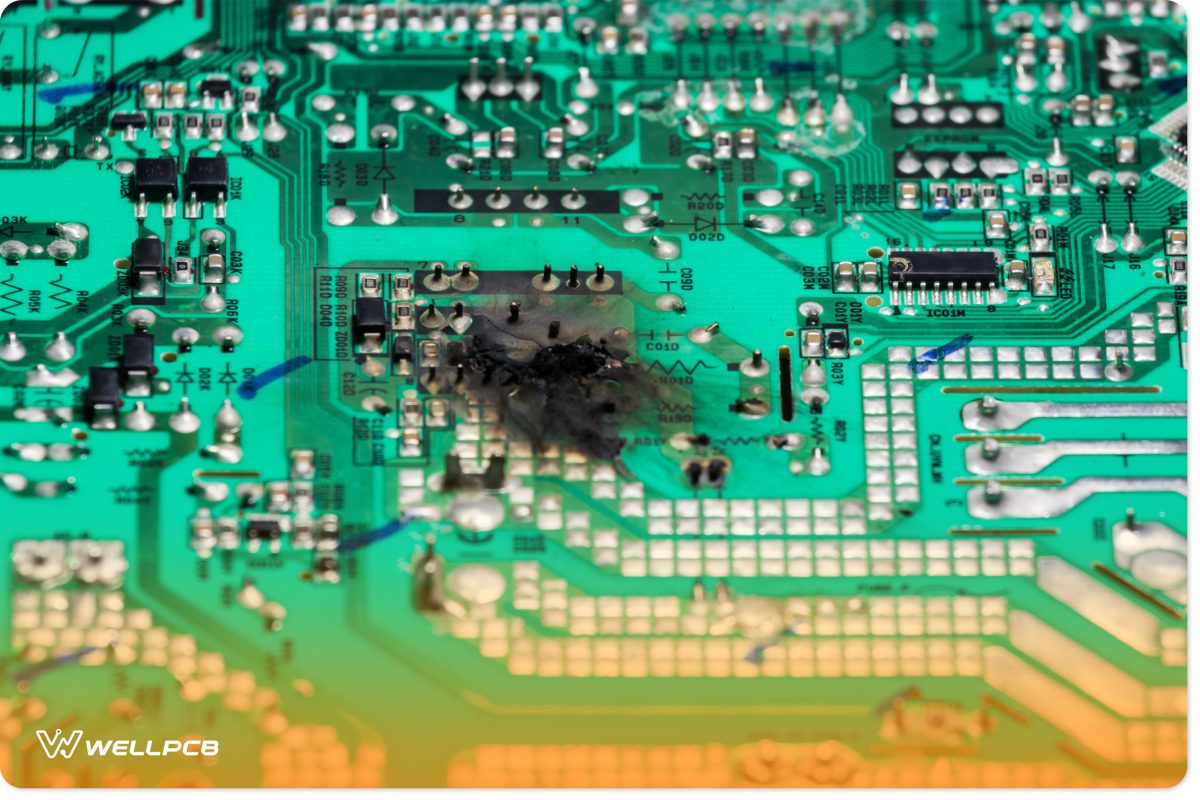
(A decomposed PCB)
Plated Through-hole Processing Equipment
Having the best, high-quality processing equipment is paramount for a manufacturing firm, among other things.
It’s essential for business success in a business, especially in this day and age of cut-throat competition. The same is true when it comes to the world of PCBs. Owning plated-through-hole processing equipment is essential.
For you to stay competitive, profitable, and relevant, such processing equipment is necessary.
The market is full of high-quality through-hole plating machines. However, you need to ensure that you source them from the right suppliers.
The Compacta 50 Through-hole plating machine is one of the best in the market so far.
The machine comes with five treatment tanks, one spray rinse tank, and two copper plating baths. It also features a 1-triple rinse that has flow control.
At all times, you need to ensure that you operate the latest plated through-hole equipment. That way, rest assured of rolling out some of the best electronic circuits.
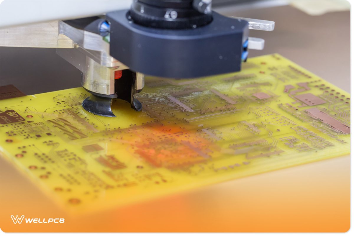
(PCB drilling machine)
Problems and Solutions of Plated Through-holes
Several significant business success accompanies plated through holes. If not addressed within the shortest time possible, then they may inhibit the functionality of the board.
Luckily enough, solutions don’t lie far away. The following plated through-hole problems and their solutions.
Blistering and lamination on board
Blistering and lamination on a circuit is a big problem for manufacturers. It is the occurrence of poor joint adhesion.
The low occurs typically because of an undesired chemical reaction of copper and the base copper.
If you want to avoid such, then make sure that you maintain cleanliness. Clean the board’s surface to improve coating and adhesion.
Also, choose a conformal coating that is less permeable. Lastly, match your conformal coating to the board’s solder and resist to get an ideal bonding.
Other causes of blistering and lamination on board include the following:
Inability to remove adhesive and oil stains
At times, you may find it hard to remove adhesives and oil pollutants, even after some rough grinding. It is another major problem that may cause blistering and lamination on the board.
If you encounter such a situation, then just know that proper pressing and drilling can solve this problem.
Such will surely strengthen or ensure that the removal of adhesive and oil stains is easy.
Neutral water is not clean after decontamination, and there is Mn on the board.
The tepid water needs to be very clean. If not, then you may end up with cases of blistering and lamination on board.
To avoid such instances, then you need to make sure that you carefully check treatment techniques. Then, if everything isn’t right, you may have to make a few adjustments.
Surfactant on the board
A surfactant is an active agent that you may find on the surface of the board. If you happen to encounter such, then it may also not be a good thing as such.
An active agent that sits on the top of the board’s surface may also result in blistering and lamination instances.
If you want to avoid such a case, you need to ensure that you factor in cleanliness.
Rinse the surface with uncontaminated water and check the density of the acid dip.
This way, you’ll be able to avoid surfactants on the board.
Insufficient roughening of copper surface
Again, short micro etching and roughening of the copper surface may lead to blistering.
It is one of those issues that face many PCB manufacturers globally.
But luckily enough, solutions don’t lie too far. If you want to avoid such, then make sure to do the following.
First, check and adjust the density, humidity, and time of the micro etching machine. At times, you may find humidity to be high in the machine.
Such may end up roughening the copper, to bring about blistering on aboard.
Tin on the copper surface
If you find a can on the copper surface, it could also spell danger. You may find a container on the body if the accelerated process is not sufficient.
Just like the previous challenge, there’s also a solution to this. Suppose you come across this problem.
Make sure that you check and adjust the accelerated process parameter. The stakes even go high if you are into large-volume production.
Surface oxidation of copper foil
Lastly, there’s surface oxidation of the copper foil. Oxidation is another issue that may result in blistering on the board.
If too much oxygen gathers in the copper foil, it will condense to form water particles. The water particles may then cause instances of blistering.
If you want to avoid such a problem, then check for the circular and dripping time. If possible, then introduce a drip system.
No copper in PTH
Insufficient copper in the plated through-hole is another PTH problem worth noting.
If there’s little to no copper in the PTH, then plating voids will arise. Plating voids on a circuit board may inhibit the adequate flow of current.
The solution for this is to ensure that sufficient copper goes to the PTH.
Again, the copper shouldn’t be in excess as such may block the holes. Other problems and solutions under this section include:
Unbalanced degreaser
If the degreaser is not balanced, you may end up with little to no copper in the PTH.
As you may well be aware, no copper in the PTH comes with many problems. If this is the case, don’t panic just yet. Carefully analyze and adjust the degreaser to the normal range.
PTH cylinder imbalance component
Do you encounter a situation where you have unbalanced ingredients in the PTH cylinder? If so, then just analyze and adjust it to the desired range.
At times, you may have to reopen the cylinder to get everything right. In some cases, you may find other ingredients depleted or too little.
Over acceleration
Excessive acceleration may result in little copper in the PTH. A solution to this is to ensure a reduction in accelerated treatment conditions.
These conditions could be aspects such as time, temperature, and density.
The drilling roughness is too large.
Is the drilling roughness excess or too large? No problem. All that you need to do is to make sure that you control the drilling. If you do so, then you’ll get the drilling roughness that you desire.
Long-term storage after PTH
There is no need to keep the board for a long time after completing the PTH. If you want everything to run smoothly, make sure you get to finish your board quickly.
According to industry experts, it’s ideal to finish the board within 8 hours after the PTH.
Fill the board with foreign matter or blister after PTH
To do this, you need to check the panel copper and high-speed circulation.
Plughole
Plugholes are necessary for the functionality of a circuit board. They prevent PCB from short-circuiting and avoid flux residue from getting to the vias.
Plugholes, when not done right, may damage the entire PHT circuit. We decided to get these to appear to be correct; proper drilling is necessary.
The following are some common Plughole challenges and their solutions.
- Resin filling – Is your drilling copper sheet or via full of resin? If so, then all that you may need to do is to control the drilling room.
- PTH cylinder copper particles – If there are some copper particles in the PTH cylinder, it may prevent copper from effectively liquidating. If you want to avoid such a scenario, then you need to check the filtering system. At times, the filtering system may be faulty or non-functional.
- Foreign matter on the panel – Panel copper residue or just foreign material on the forum may be problematic. Undertaking carbon treatment on time is necessary. It will shield the plate from burning from the copper powder that drops.
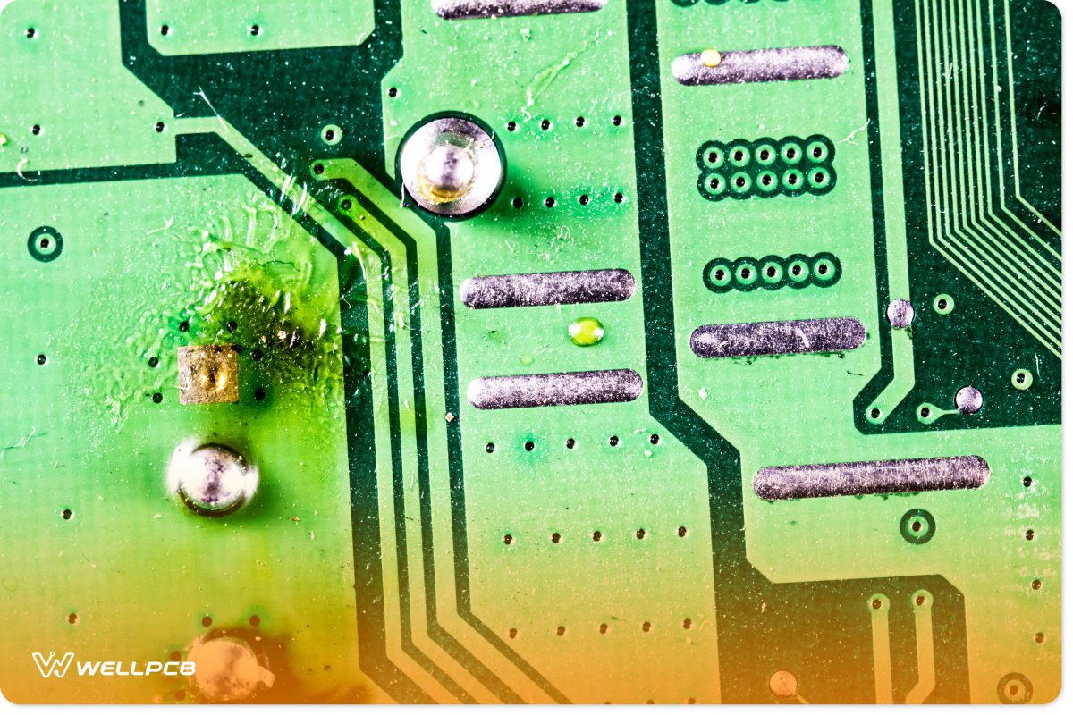
(Damaged Plugholes of a PCB)
Summary
Plated through-hole technology is here with us. And as things look, PTH is here to stay. But on the brighter side, it comes with plenty of advantages.
PTH is excellent for prototyping and testing. Here, you’re able to swap components on the PCB before designing the breadboard efficiently.
As noted before, through-hole components are robust, assuring you of durability. Do you have any upcoming PTH projects?
We deliver unprecedented amounts of integration to the electronics industry. The design of the PTH PCBs requires technical skills and precision.
If you are planning to have high-quality boards, then there’s no harm in approaching industry experts. Call us today for all your PTH PCB solutions.


