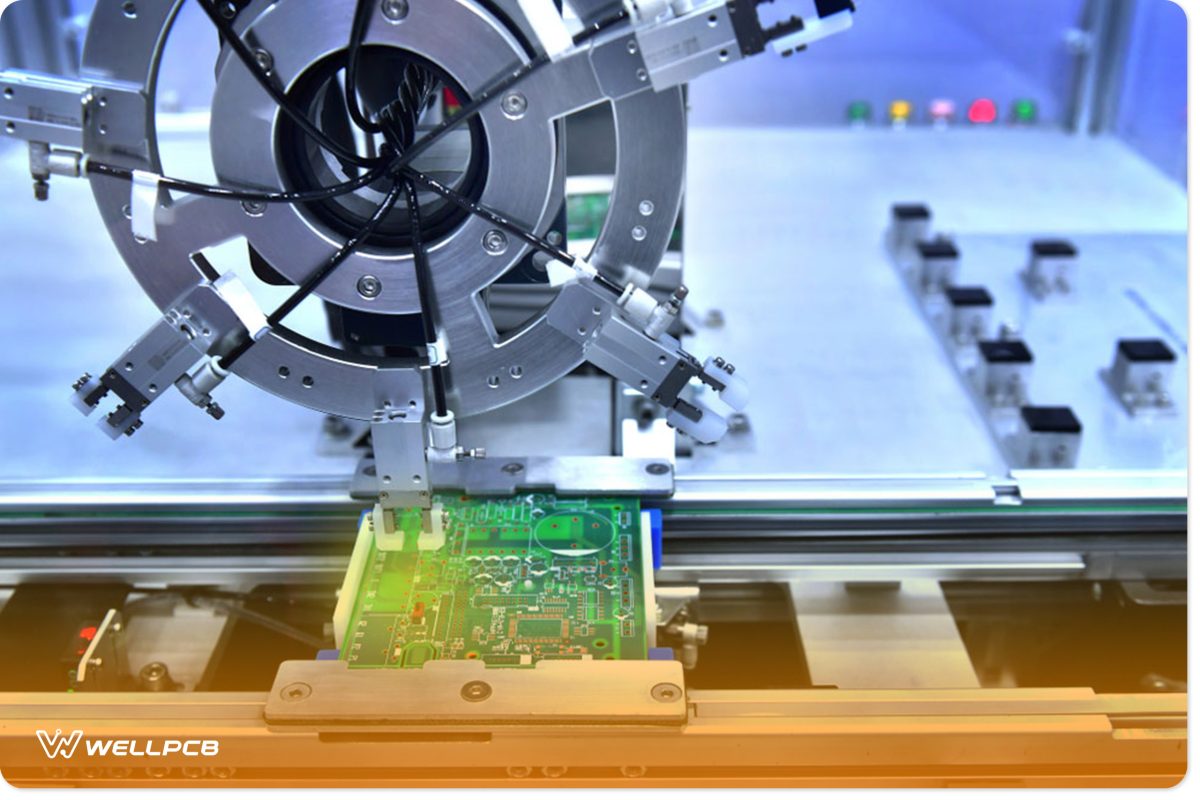
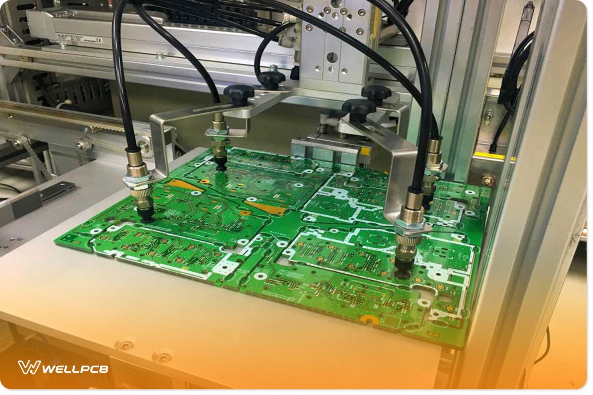
It is important to remember that the milling accuracy and control and the sharpness of the milling bits determine the quality of the board.
PCB milling allows for prototyping and creating unique PCB designs. When milling, a single machine may perform the required action to create a prototype board.
The engine uses the standard AC supply and vacuum cleaner for smooth operation.

The mechanics behind the milling machine are straightforward. It is miniature and entirely accurate.
The device can easily be controlled by software via commands sent.
The controller should then monitor the positioning of the components as he moves the milling head.
This helps to maintain the spindle speed, which ranges from 30,000 RPM to 100,000 RPM.
Notice that the higher the spindle speed, the greater the accuracy.
.

The PCB milling machine utilizes the stepper motor to drive the precision of the X and Y axis system.
A unique precision connection assembly may be used to ensure alignment in the milling.
Milling PCBs come with a lot of challenges, including handling variations in flatness.
This is because etching techniques use optical masks that sit on the copper layer and conform to slight bends in the material to ensure that all features are replicated.
However, when you mill, the minute height variation causes the sinking or rising of con-shaped bits. Therefore, it may be necessary that mapping is done to help adjust the Z values beforehand.


